

To control junction depth in transistors, precise quantities of impurities are introduced at relatively shallow depths by
Question:
To control junction depth in transistors, precise quantities of impurities are introduced at relatively shallow depths by ion implantation and diffused into the silicon substrate in a subsequent thermal treatment. This can be approximated as a finite source diffusion problem. Applying the appropriate boundary conditions, the solution to Fick’s second law under these conditions is
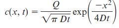
where Q is the initial surface concentration with units of atoms/cm2. Assume that we implant 1014 atoms/cm2 of phosphorus at the surface of a silicon wafer with a background boron concentration of 1016 atoms/ cm3 and this wafer is subsequently annealed at 1100°C. The diffusion coefficient of phosphorus in silicon at 1100°C is 6.5 x 10⁻¹³ cm2/s.
(a) Plot a graph of the concentration c (atoms/cm3) versus x (cm) for anneal times of 5 minutes, 10 minutes, and 15 minutes.
(b) What is the anneal time required for the phosphorus concentration to equal the boron concentration at a depth of 1 μm?
Step by Step Answer:
a To plot a graph of the concentration c atomscm3 versus x cm for anneal times of 5 minutes 10 minut...View the full answer


The Science And Engineering Of Materials
ISBN: 9781305076761
7th Edition
Authors: Donald R. Askeland, Wendelin J. Wright
