

A BiCMOS Class AB output stage is shown in Fig. 5.43. Device parameters are β F (npn)
Question:
(a) Calculate bias currents in all devices for Vo = 0.
(b) Calculate the positive and negative limits of Vo for RL = 200 Ω. Thus calculate the maximum average power that can be delivered to RL before clipping occurs.
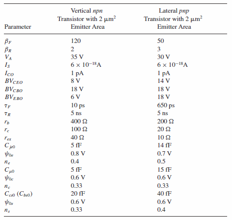
(c) Use SPICE to check (a) and also to plot the complete dc transfer characteristic of the circuit from Vi to Vo. Also plot the waveforms of Ic1, Ic2, and Id2 for a sinusoidal output voltage at Vo of 2 V and then 4 V zero-to-peak. In the simulation, assume bipolar parameters as in Fig. 2.32 and MOS parameters as in Table 2.3 (apart from the values of βF and μpCox given above).
Figure 5.43:
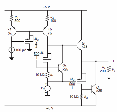
Fig. 2.32:
Fantastic news! We've Found the answer you've been seeking!
Step by Step Answer:
a Bias V o 0 I C5 100 A I C6 500 A I D3 I B5 I B6 600 A20 30 A I C3 500 80 420 A From KVL V GS...View the full answer

Answered By
Joseph Mwaura
I have been teaching college students in various subjects for 9 years now. Besides, I have been tutoring online with several tutoring companies from 2010 to date. The 9 years of experience as a tutor has enabled me to develop multiple tutoring skills and see thousands of students excel in their education and in life after school which gives me much pleasure. I have assisted students in essay writing and in doing academic research and this has helped me be well versed with the various writing styles such as APA, MLA, Chicago/ Turabian, Harvard. I am always ready to handle work at any hour and in any way as students specify. In my tutoring journey, excellence has always been my guiding standard.
1+ Reviews
10+ Question Solved
Related Book For 
Analysis and Design of Analog Integrated Circuits
ISBN: 978-0470245996
5th edition
Authors: Paul R. Gray, Paul J. Hurst Stephen H. Lewis, Robert G. Meyer
Question Posted:
