

Question: (a) Calculate the random input offset voltage for the op amp in Fig. 6.16. Assume the matching is perfect except thatV t3 V t4 =
(b) Repeat (a) for an op amp that uses an n-channel differential pair and a p-channel current-mirror load.
(c) Which of these two configurations gives lower input offset voltage? Explain
Figure 6.16
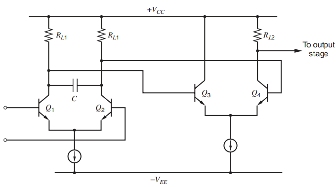
Table 2.4
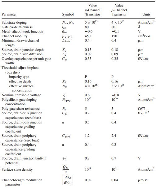
+Vcc R12 To output stage RL1 R11 Q4 Q3 Q2 Q1 -VEE Value Value n-Channel p-Channel Parameter Symbol Transistor Transistor Units Substrate doping NA, ND 5 x 10⁵ 4 x 10¹⁶ Atoms/cm Gate oxide thickness lox 80 80 -0.1 150 Metal-silicon work function -0.6 cm?/V-s Channel mobility Minimum drawn channel length Source, drain junction depth Source, drain side diffusion Overlap capacitance per unit gate 450 Larwn 0.4 0.4 um X} La Cd 0.15 0.18 um 0.09 0.09 um 0.35 0.35 fF/um width Threshold adjust implant (box dist) impurity type effective depth effective surface , 0.16 0.16 pm 4 x 10¹⁶ 3 x 10¹⁶ Atoms/cm concentration Nominal threshold voltage Polysilicon gate doping concentration V, Napoly 0.6 100 -0.8 100 Atoms/cm R, Poly gate sheet resistance Source, drain-bulk junction Cp 0.2 0.4 fF/um? capacitances (zero bias) Source, drain-bulk junction capacitance grading coefficient 0.5 0.4 Source, drain periphery capacitance (zero bias) Source, drain periphery 1.2 2.4 fF/um 0.4 0.3 capacitance grading coefficient Source, drain junction built-in potential 0.7 0.7 Os Surface-state density 10" 10" Atoms/cm d Channel-length modulation 0.02 0.04 um/V dVps parameter
Step by Step Solution
3.45 Rating (168 Votes )
There are 3 Steps involved in it
From 669 From 118 with WL 3 WL 1 And I D1 I D... View full answer

Get step-by-step solutions from verified subject matter experts
Document Format (2 attachments)
1528_605d88e1b4430_686888.pdf
180 KBs PDF File
1528_605d88e1b4430_686888.docx
120 KBs Word File