

Question: A differential circuit employing active loads is shown in Fig. 7.42. Bias voltage V B is adjusted so that the collectors of Q 1 and
A differential circuit employing active loads is shown in Fig. 7.42. Bias voltage VBis adjusted so that the collectors of Q1and Q2are at +5 V dc. Biasing resistors are RB1= 10 kΩ and RB2= 20 kΩ. Calculate the low-frequency, small-signal voltage gain Ï…o/Ï…i, and use the zero-value time-constant method in the DM half-circuit to estimate the ˆ’3-dB frequency of the DM gain. Use the device data in Problem 7.25.
Data from Prob. 7.25:
Data: npn: β = 100, fT = 500 MHz at IC = 1 mA, Cμ0 = 0.7 pF, Cje = 3 pF (at the bias point), Ccs0 = 2 pF, rb = 0, and VA = 120 V. Assume n = 0.5 and ψ0 = 0.55 V for all junctions. pnp: β = 50, fT = 4 MHz at IC = ˆ’0.5 mA, Cμ0 = 1.0 pF, Cje = 3 pF (at the bias point), Cbs0 = 2 pF, rb = 0, and |VA| = 50 V. Assume n = 0.5 and ψ0 = 0.55 V for all junctions.
Fig. 7.42:
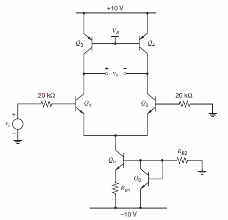
+10 V VR Q4 o Vo 20 k2 20 k2 O2 w- Rg2 O5 RB1 -10 V
Step by Step Solution
3.45 Rating (164 Votes )
There are 3 Steps involved in it
Halfcircuits ac Equivalent 10 A I C1 I C3 I C5 2 5 A Q 1 122 pF at 1 mA C 1 12 pF at 1 m... View full answer

Get step-by-step solutions from verified subject matter experts
Document Format (2 attachments)
1528_605d88e1b9317_686935.pdf
180 KBs PDF File
1528_605d88e1b9317_686935.docx
120 KBs Word File