

Question: Repeat Problem 7.25 with the following changes: 1. Replace Q 1 with a p-channel MOS transistor, M 1 . Replace Q 2 and Q 3
1. Replace Q1 with a p-channel MOS transistor, M1. Replace Q2 and Q3 with n-channel MOS transistors, M2 and M3.
2. Add a resistor of value 1/gm1 from the gate to the source of M1.
3. Take VSUPPLY = 2.5 V.
4. Use the formula for Cdb0 given in Problem 7.17.
5. For all transistors: Ldrwn = 2 µm, Ld = 0.2 µm, Xd = 1 µm, and γ = 0. W1 = 200 µm and W2 =
W3 = 100 µm. Use (1.201) and (1.202) with ψ0 = 0.6 V for the junction capacitances. Use the equations in Problem 7.17 for Cdb0. NMOS data: Vtn = 1 V, k€™n = 60 µA/V2, λn = 1/(100 V), Cox = 0.7 fF/(µm2), Cj0 = 0.4 fF/(µm2), and Cjsw0 = 0.4 fF/µm. PMOS data: Vtp = ˆ’1 V, k€™p = 20 µA/V2, |λp| = 1/(50 V), Cox = 0.7 fF/(µm2), Cj0 = 0.2 fF/(µm2), and Cjsw0 = 0.2 fF/µm.
Data from Prob. 7.25:
An amplifier stage is shown in Fig. 7.41 where bias current IB is adjusted so that VO = 0 V dc. Take VSUPPLY = 10 V.
(a) Calculate the low-frequency, small-signal trans-resistance Ï…o/ii and use the zero-value time-constant method to estimate the ˆ’3-dB frequency. Data: npn: β = 100, fT = 500 MHz at IC = 1 mA, Cμ0 = 0.7 pF, Cje = 3 pF (at the bias point), Ccs0 = 2 pF, rb = 0, and VA = 120 V. Assume n = 0.5 and ψ0 = 0.55 V for all junctions. pnp: β = 50, fT = 4 MHz at IC = ˆ’0.5 mA, Cμ0 = 1.0 pF, Cje = 3 pF (at the bias point), Cbs0 = 2 pF, rb = 0, and |VA| = 50 V. Assume n = 0.5 and ψ0 = 0.55 V for all junctions.
(b) Repeat (a) if a 20-pF capacitor is connected from collector to base of Q1.
Fig. 7.41:
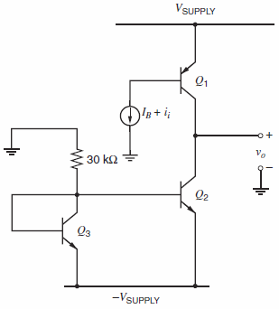
VSUPPLY )'s + i; 'a + 30 k2 Q2 Q3 -VSUPPLY
Step by Step Solution
3.51 Rating (164 Votes )
There are 3 Steps involved in it
Interate to find the bias current start with V ov3 0 Still V ov3 ... View full answer

Get step-by-step solutions from verified subject matter experts
Document Format (2 attachments)
1528_605d88e1b90db_686934.pdf
180 KBs PDF File
1528_605d88e1b90db_686934.docx
120 KBs Word File