

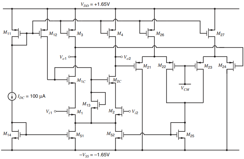
Question: A fully differential op amp with CMFB is shown in Fig. 12.57. For M 1 , M 1C , M 2 , and M 2C
A fully differential op amp with CMFB is shown in Fig. 12.57. For M1, M1C, M2, and M2C, use W/L = (64 µm) / (0.8 µm). For M3 €“ M4, M26 €“ M27and M11, W / L = (96 µm) / (1.4 µm). For M21€“ M24, W / L = (6 µm) / (0.8 µm). For M14, M25, and M52, W / L = (16 µm) / (0.8 µm). For M13, W / L = (1.4 µm) / (0.8 µm). Take VCM = ˆ’0.65 V.
(a) Choose W values for M12 and M51 so that |ID13|=20 µA. Use L = 0.8 µm for M51 and L = 1.4 µm for M12.
(b) Use SPICE to find the low-frequency op-amp gains vod /vid, voc/vic, vod/vic, and voc/vid with the CMFB active.
(c) Calculate the output slew rate dVod/dt if a 4-pF capacitor is connected from each op-amp output to ground.
(d) What is the differential output voltage swing of this op amp? Assume Vic = VCM, and ignore body effect for this calculation.
(e) Repeat (b) when the input transistors are mismatched with W1 = 63 µm and W2 = 65 µm. (Note: With mismatch, the op-amp offset voltage is not zero.)
(f) Repeat (b) when the load transistors are mismatched with W3 = 95 µm and W4 = 97 µm.
Figure 12.57:
VDp = +1.65V %3D M27 M26 M4 M12 M11 Vo2 M24 M23 Vo1 M22 M21 M2C M1C V I 3 100 M13 M2o Vi2 M1 V;1 M25 M52 M51 M14 -Vss =-1.65V
Step by Step Solution
3.34 Rating (169 Votes )
There are 3 Steps involved in it
a I D51 I D1 I D2 I D13 I D52 100 100 20 100 120 A I D12 I D13 2... View full answer

Get step-by-step solutions from verified subject matter experts