

Question: A variable-gain CMOS amplifier is shown in Fig. 8.52. Note that M 4 represents shunt feedback around M 6 . Assuming that the bias value
Fig. 8.52:
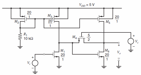
VDp = 5 V 20 M3, 20 20 M2 M5 R1 M4. 10 k2 2 Ve |M6 20 M1 20 Vo
Step by Step Solution
★★★★★
3.26 Rating (152 Votes )
There are 3 Steps involved in it
1 Expert Approved Answer
Step: 1 Unlock

5 a 3 a 08 2 3 a 2 48 a 192 0 3 a 2 38 a 308 V GS2 183 V 317 A I ... View full answer
Question Has Been Solved by an Expert!
Get step-by-step solutions from verified subject matter experts
Step: 2 Unlock
Step: 3 Unlock
Document Format (2 attachments)
1528_605d88e1c8ff3_687108.pdf
180 KBs PDF File
1528_605d88e1c8ff3_687108.docx
120 KBs Word File