

Question: A CMOS amplifier stage is shown in Fig. 7.49. Select W/L for M 1 and M 5 to give V i = V O =
A CMOS amplifier stage is shown in Fig. 7.49. Select W/L for M1and M5to give Vi= VO= 2.5V dc and |ID| = 100 µA bias in all devices. The minimum value of L and W is 2 µm. Calculate the small-signal, low-frequency gain and the ˆ’3-dB frequency of the stage. Verify with SPICE. Use device data from Problem 7.37(a) with |λ| = 0.03 Vˆ’1, μpCox= 30 µA/V2, and Vtp= ˆ’0.7 V.
Data from Prob. 7.37:
A wideband MOS amplifier stage is shown in Fig. 7.48. Calculate the small-signal, low-frequency gain and use the zero-value time constant method to estimate the ˆ’3-dB bandwidth. Use μnCox = 60 µA/V2, tox = 20 nm, Col = 0.3 fF/(µm of gate width), ψo = 0.6 V, Vt = 0.7 V, γ = 0.4 V1/2, λ = 0, and VO = 2.5 V dc. For Cdb and Csb, use Cdb0 = Csb0 =0.8 fF/(µm of gate width).
Fig. 7.49:
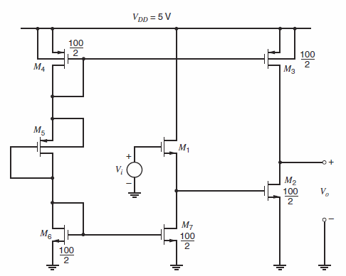
VDp = 5 V 100 100 M4 M3 M5 M1 M2 100 M7 M5 100 100 2
Step by Step Solution
3.34 Rating (163 Votes )
There are 3 Steps involved in it
100 15 50 V GS V t 2 V GS 1065 V m 2 m 6 m 7 100 30 50 V ... View full answer

Get step-by-step solutions from verified subject matter experts
Document Format (2 attachments)
1528_605d88e1baa75_686947.pdf
180 KBs PDF File
1528_605d88e1baa75_686947.docx
120 KBs Word File