

Question: Determine the input offset voltage of the source-coupled pair in Fig. 3.50 for which I TAIL = 50 µA. The drawn device dimensions are W
Fig. 3.50:
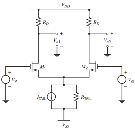
Table 2.4:
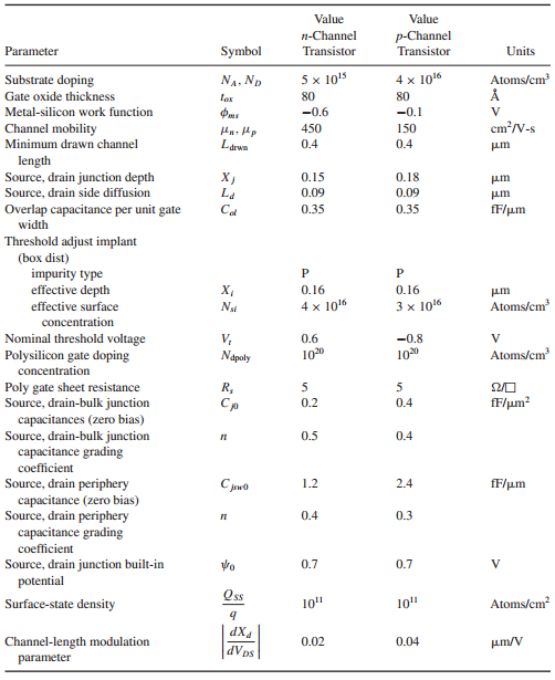
+Vpp Rp Rp Vo2 Vo1 M2 M1 Vi2 Vi1 RTAIL ITAIL -Vss Value Value n-Channel p-Channel Parameter Symbol Transistor Transistor Units Substrate doping Gate oxide thickness 5 x 10⁵ 4 x 10¹⁶ NA, ND Atoms/cm lox 80 80 Metal-silicon work function -0.6 -0.1 450 cm?/V-s Channel mobility Minimum drawn channel length Source, drain junction depth Source, drain side diffusion 150 Larwn 0.4 0.4 um X) L4 0.15 0.18 um 0.09 0.09 um Overlap capacitance per unit gate 0.35 0.35 fF/um width Threshold adjust implant (box dist) impurity type effective depth effective surface , 0.16 4 x 10¹⁶ 0.16 Nsi 3 x 10¹⁶ Atoms/cm concentration Nominal threshold voltage Polysilicon gate doping concentration V, Napoly 0.6 100 -0.8 100 Atoms/cm Poly gate sheet resistance Source, drain-bulk junction R, Cp 0.2 0.4 fF/um? capacitances (zero bias) Source, drain-bulk junction capacitance grading 0.5 0.4 coefficient Source, drain periphery capacitance (zero bias) Source, drain periphery 1.2 2.4 fF/um 0.4 0.3 capacitance grading coefficient Source, drain junction built-in potential 0.7 0.7 Os Surface-state density 101 10" Atoms/cm , Channel-length modulation parameter 0.02 0.04 um/V dV ps
Step by Step Solution
3.33 Rating (186 Votes )
There are 3 Steps involved in it
From 3248 L eff 1 2 009 082 m If WL 1 ... View full answer

Get step-by-step solutions from verified subject matter experts
Document Format (2 attachments)
1528_605d88e1ac2cb_686810.pdf
180 KBs PDF File
1528_605d88e1ac2cb_686810.docx
120 KBs Word File