

Question: Repeat Problem 4.16 except replace the npn and pnp transistors with n-channel and p-channel MOS transistors, respectively. Assume W n = 50[1]µm and W p
Table 2.3:
Repeat Problem 4.16:
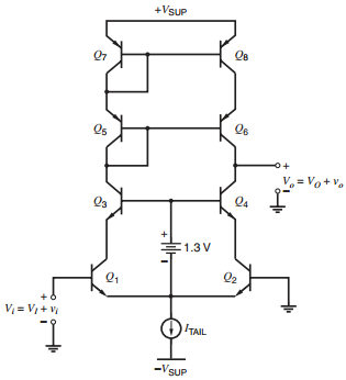
Determine the unloaded voltage gain νo/νi and output resistance for the circuit of Fig. 4.59. Neglect rμ. Verify with SPICE and also use SPICE to plot the large-signal VO-VI transfer characteristic for VSUP = 2.5V.
Figure 4.59:
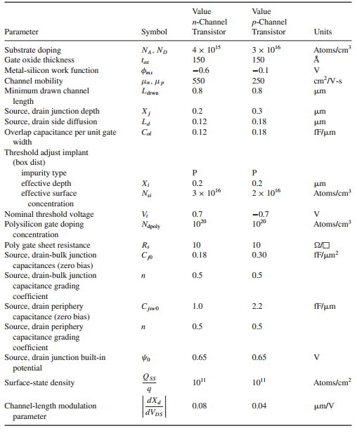
Value Value p-Channel Transistor n-Channel Units Parameter Symbol Transistor NA, ND 4 x 10⁵ Substrate doping Gate oxide thickness 3 x 10¹⁶ Atoms/cm 150 150 fax Metal-silicon work function -0.6 -0.1 cm?/V-s Channel mobility Minimum drawn channel 550 250 Lawn 0.8 0.8 um length Source, drain junction depth Source, drain side diffusion Overlap capacitance per unit gate width X, 0.2 0.3 um 0.18 0.12 um Cad 0.12 0.18 fF/um Threshold adjust implant (b dist) impurity type effective depth effective surface XI 0.2 0.2 um Atoms/cm 3 x 10¹⁶ 2 x 10¹⁶ concentration Nominal threshold voltage Polysilicon gate doping concentration 0.7 -0.7 Atoms/cm 100 Napoly 100 Poly gate sheet resistance Source, drain-bulk junction capacitances (zero bias) Source, drain-bulk junction Rs 10 10 fF/um? Co 0.18 0.30 0.5 0.5 capacitance grading coefficient Source, drain periphery capacitance (zero bias) Source, drain periphery capacitance grading 1.0 2.2 fF/um 0.5 0.5 coefficient Source, drain junction built-in potential 0.65 0.65 Oss Atoms/cm? Surface-state density 10" 101 dX4 Channel-length modulation 0.08 0.04 um/V dVps parameter +VSUP Os Vo+v Q4 1.3 V Q2 V = V + V ITAIL -VSUP
Step by Step Solution
3.38 Rating (170 Votes )
There are 3 Steps involved in it
R o gm 6 r 06 r 08 gm 4 r 04 r 02 r 06 r 08 1650 320 k r 04 r 02 ... View full answer

Get step-by-step solutions from verified subject matter experts
Document Format (2 attachments)
1528_605d88e1ae790_686829.pdf
180 KBs PDF File
1528_605d88e1ae790_686829.docx
120 KBs Word File