

Question: We can convert all load/store instructions into register-based (no offset) and put the memory access in parallel with the ALU. What is the clock cycle
We can convert all load/store instructions into register-based (no offset) and put the memory access in parallel with the ALU. What is the clock cycle time if this is done in the single-cycle and in the pipelined datapath? Assume that the latency of the new EX/MEM stage is equal to the longer of their latencies.
Each pipeline stage in Figure 4.33 has some latency. Additionally, pipelining introduces registers between stages, and each of these adds an additional latency. The remaining problems in this exercise assume the following latencies for logic within each pipeline stage and for each register between two stages: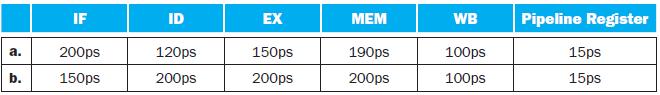
Figure 4.33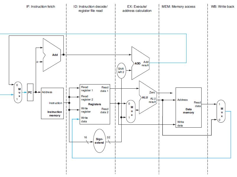
a. b. IF 200ps 150ps ID 120ps 200ps EX 150ps 200ps MEM 190ps 200ps WB 100ps 100ps Pipeline Register 15ps 15ps
Step by Step Solution
3.44 Rating (163 Votes )
There are 3 Steps involved in it
For the pipelined datapath each stage operates in paral... View full answer

Get step-by-step solutions from verified subject matter experts