

Question: Write an HDL module for the circuit in Exercise 3.34. You may use the full adder from Section 4.2.5. Data from problem 3.34 You are
Write an HDL module for the circuit in Exercise 3.34. You may use the full adder from Section 4.2.5.
Data from problem 3.34
You are designing an adder for the blindingly fast 2-bit RePentium Processor. The adder is built from two full adders such that the carry out of the first adder is the carry in to the second adder, as shown in Figure 3.75. Your adder has input and output registers and must complete the addition in one clock cycle. Each full adder has the following propagation delays: 20 ps from Cin to Cout or to Sum (S), 25 ps from A or B to Cout, and 30 ps from A or B to S. The adder has a contamination delay of 15 ps from Cin to either output and 22 ps from A or B to either output. Each flip-flop has a setup time of 30 ps, a hold time of 10 ps, a clockto-Q propagation delay of 35 ps, and a clock-to-Q contamination delay of 21 ps.
(a) If there is no clock skew, what is the maximum operating frequency of the circuit?
(b) How much clock skew can the circuit tolerate if it must operate at 8 GHz?
(c) How much clock skew can the circuit tolerate before it might experience a hold time violation?
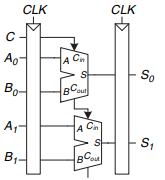
CLK CLK Ao- Cn So Bo- Cou A,- 1A B1- BCu out
Step by Step Solution
3.53 Rating (173 Votes )
There are 3 Steps involved in it
SystemVerilog VHDL module ex445 inpu... View full answer

Get step-by-step solutions from verified subject matter experts