

Question: Write an HDL module for the circuit in Exercise 3.33 Data from problem 3.33 Ben Bitdiddle has designed the circuit in Figure 3.74 to compute
Write an HDL module for the circuit in Exercise 3.33
Data from problem 3.33
Ben Bitdiddle has designed the circuit in Figure 3.74 to compute a registered four-input XOR function. Each two-input XOR gate has a propagation delay of 100 ps and a contamination delay of 55 ps. Each flip-flop has a setup time of 60 ps, a hold time of 20 ps, a clock-to-Q maximum delay of 70 ps, and a clock-to-Q minimum delay of 50 ps.
(a) If there is no clock skew, what is the maximum operating frequency of the circuit?
(b) Alyssa P. Hacker points out that she can redesign the combinational logic between the registers to be faster and tolerate more clock skew. Her improved circuit also uses three two-input XORs, but they are arranged differently. What is her circuit? What is its maximum frequency if there is no clock skew? How much clock skew can the circuit tolerate before it might experience a hold time violation?
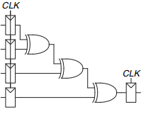
CLK CLK
Step by Step Solution
3.47 Rating (186 Votes )
There are 3 Steps involved in it
a SystemVerilog VHDL b SystemVe... View full answer

Get step-by-step solutions from verified subject matter experts