

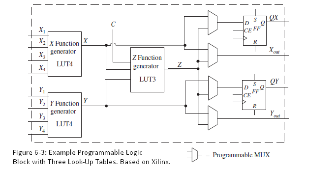
Question: (a) Write Verilog code that describes the logic block shown in Figure 6-3. Use a module similar to that used in Problem 6.6(a), except add
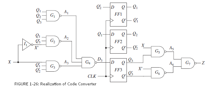
(b) Write structural Verilog code that instantiates two Figure 6-3 block components to implement the code converter shown in Figure 1-26. When you instantiate a block component, use the actual bit patterns stored in XLUT, YLUT, and ZLUT to specify the function generated by each of the LUTs.
Data from Problem 6.6.
Write Verilog code that describes the logic block shown in Figure 6-1(a). Use
the following module:
module Figure6_1a(X_in,Y_in,clk,CE,Qx,Qy,X,Y,XLUT,YLUT);
input[1:4]X_in,Y_in;
input CE,clk;
input[0:15] XLUT,YLUT;
inout X,Y;
output Qx,Qy;
.
.
.
endmodule
Q2 Qi G Q2 A1 FF1 Q1- Qi Q3 G2 FF2 Q'FQ2 X' A5 G5 | 23 D3 G4 A A Qi G3 X' FF3 G6 Q3 Q' CLK FIGURE 1-26: Realization of Code Converter QX , CE FF X2 |X Function X generator X3 Z Function LUT4 | X4 generator LUT3 | Y1 QY D. FF CE |Y2 Y Function Y generator Y3 LUT4 Yout | Y4 Figure 6-3: Example Programmable Logic Block with Three Look-Up Tables. Based on Xilinx. Programmable MUX
Step by Step Solution
3.24 Rating (162 Votes )
There are 3 Steps involved in it
a module Figure63Xin Yin clk CE C Qx Qy X Y XLUT YLUT ZLUT SA SB SC SD inpu... View full answer

Get step-by-step solutions from verified subject matter experts