

Question: An 8-bit right-shift register with parallel load is to be implemented using an FPGA with logic blocks as shown in Figure 6-1(a). The flip-flops are
(a) How many logic blocks are required?
(b) Show the required connections for the rightmost block on a copy of Figure 6-1(a). Connect N to CE.
(c) Give the function generator outputs for this block.
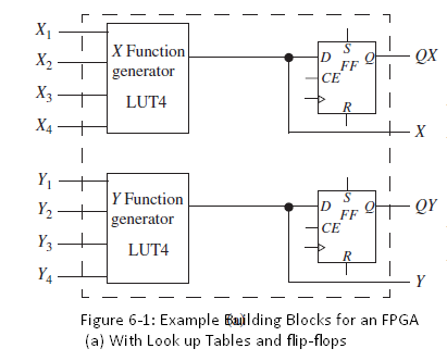
X1 | X2 X Function FF CE generator X3 LUT4 X4 Y1 Y Function QY D. FF CE generator Y3 LUT4 Y4 Figure 6-1: Example Bailding Blocks for an FPGA (a) With Look up Tables and flip-flops
Step by Step Solution
★★★★★
3.43 Rating (162 Votes )
There are 3 Steps involved in it
1 Expert Approved Answer
Step: 1 Unlock

a 4 Cells if N is used as the clock enable When N 1 t... View full answer
Question Has Been Solved by an Expert!
Get step-by-step solutions from verified subject matter experts
Step: 2 Unlock
Step: 3 Unlock