

The propagation delay through the combinational circuit in Figure 5.2 is 600 ps (picoseconds). The registers have
Fantastic news! We've Found the answer you've been seeking!
Question:
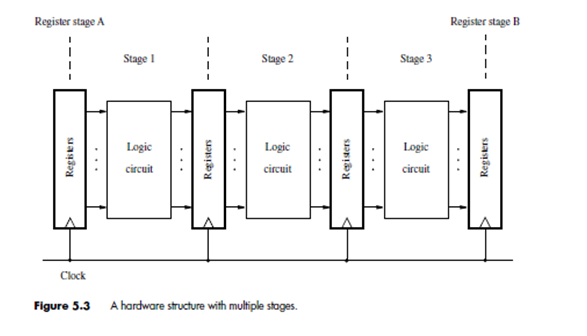
The propagation delay through the combinational circuit in Figure 5.2 is 600 ps (picoseconds). The registers have a setup propagation delay from the clock input to the 0 outputs is 70 ps. (a) What is the minimum clock period required for correct operation of this circuit? (b) Assume that the circuit is reorganised into three stages as in Figure 5.3, such that the combinational circuit in each stage has a delay of 200 ps. What is the minimum clock period in this case? Reference of Fig.5.2
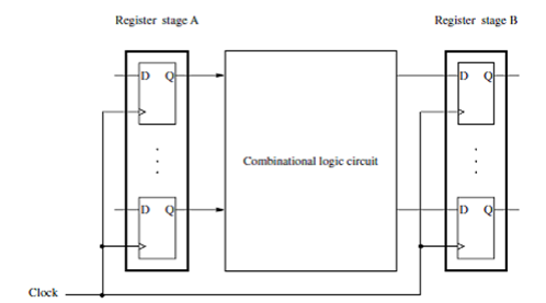
Figure 5.3
Expert Answer:

Related Book For 

Digital Systems Design Using Verilog
ISBN: 978-1285051079
1st edition
Authors: Charles Roth, Lizy K. John, Byeong Kil Lee
Posted Date:
