

Question: 1. Consider the full-wave phase-controlled rectifier circuit of Fig. Pl.1 and supplied from an ac source of v(t) = 110 sin 377t and with
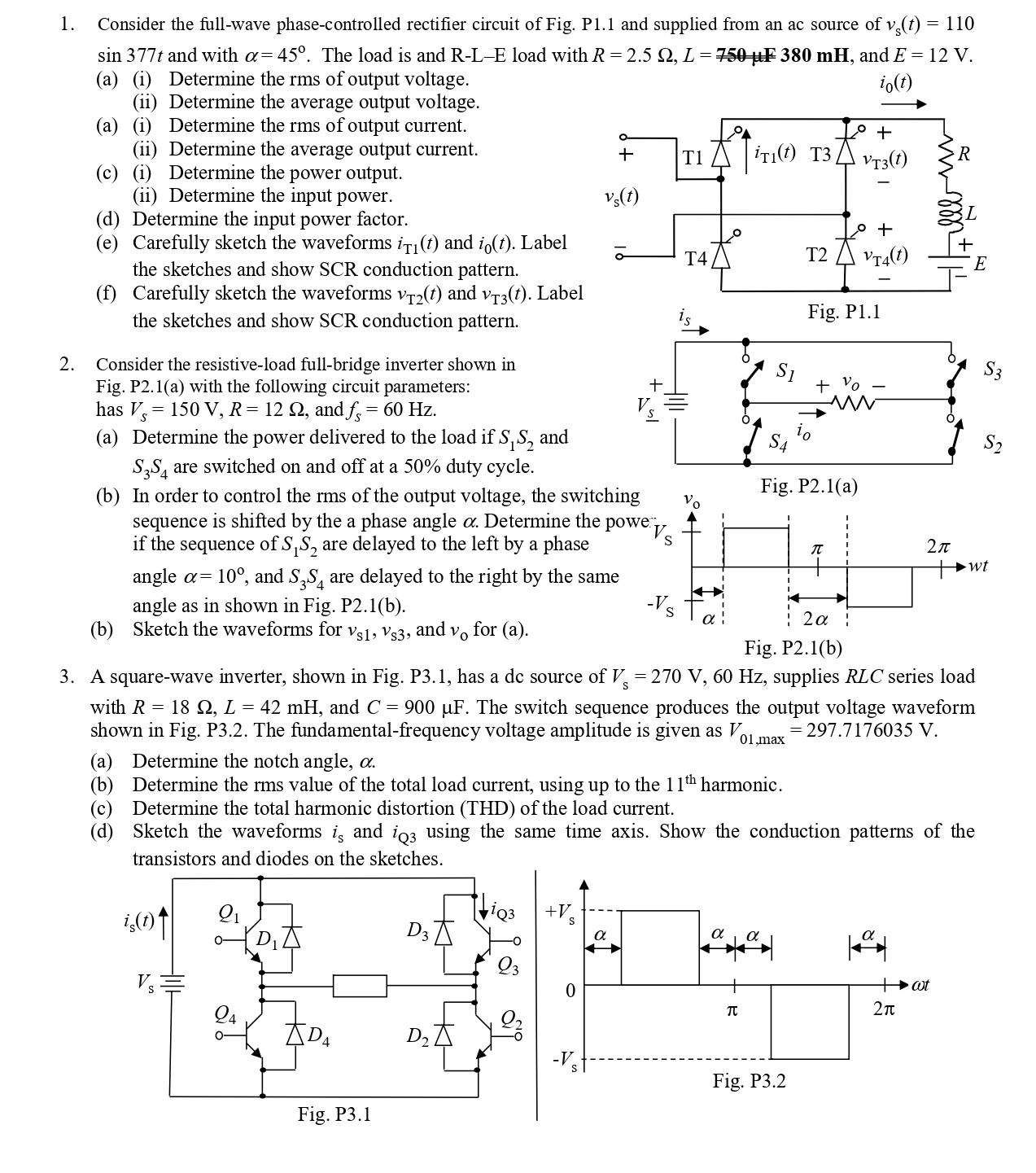
1. Consider the full-wave phase-controlled rectifier circuit of Fig. Pl.1 and supplied from an ac source of v(t) = 110 sin 377t and with a= 45. The load is and R-L-E load with R=2.5 92, L= 750 F 380 mH, and E = 12 V. (a) (i) Determine the rms of output voltage. io(t) (ii) Determine the average output voltage. (a) (i) Determine the rms of output current. (ii) Determine the average output current. 2. (c) (i) Determine the power output. (ii) Determine the input power. (d) Determine the input power factor. (e) Carefully sketch the waveforms it (t) and io(t). Label the sketches and show SCR conduction pattern. (f) Carefully sketch the waveforms V1(t) and vT3(t). Label the sketches and show SCR conduction pattern. Consider the resistive-load full-bridge inverter shown in Fig. P2.1(a) with the following circuit parameters: has V, 150 V, R = 12 Q2, and f = 60 Hz. = (a) Determine the power delivered to the load if S S and S3S are switched on and off at a 50% duty cycle. (b) In order to control the rms of the output voltage, the switching sequence is shifted by the a phase angle a. Determine the if the sequence of SS, are delayed to the left by a phase 2 angle a = 10, and SS are delayed to the right by the same angle as in shown in Fig. P2.1(b). Sketch the waveforms for vs1, Vs3, and Vo for (a). D.D Fig. P3.1 D iQ3 23 + vs(t) Si -V + powe a Vs Vs -Vs T1 T4 iT1(1) T3 S1 I T2 Fig. P3.2 io Fig. P2.1(a) + Vo 2 (b) Fig. P2.1(b) S 3. A square-wave inverter, shown in Fig. P3.1, has a de source of V = 270 V, 60 Hz, supplies RLC series load with R 18 2, L= 42 mH, and C= 900 F. The switch sequence produces the output voltage waveform shown in Fig. P3.2. The fundamental-frequency voltage amplitude is given as Vo = 297.7176035 V. (a) Determine the notch angle, a. 01,max (b) Determine the rms value of the total load current, using up to the 11th harmonic. (c) Determine the total harmonic distortion (THD) of the load current. (d) Sketch the waveforms is and i93 using the same time axis. Show the conduction patterns of the transistors and diodes on the sketches. i(t) + Fig. P1.1 VT3(t) + VT4(t) 2 R +at 2 E wt
Step by Step Solution
3.33 Rating (156 Votes )
There are 3 Steps involved in it
1 The rms of output voltage can be calculated using the formula for the rms value of a rectified sinusoidal waveform which is Vrms 09 Vpeak where Vpeak is the peak voltage of the input sinusoidal wave... View full answer

Get step-by-step solutions from verified subject matter experts