

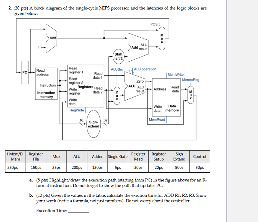
Question: 2 . ( 2 0 pts ) A block diagram of the single - cycle MIPS processor and the latencies of the logic blocks are
pts A block diagram of the singlecycle MIPS processor and the latencies of the logic blocks are given below.
begintabularcccccccccc
hline begintabularc
IMemD
Mem
endtabular & begintabularc
Register
File
endtabular & Mux & ALU & Adder & Single Gate & begintabularc
Register
Read
endtabular & begintabularc
Register
Setup
endtabular & begintabularc
Sign
Extend
endtabular & Control
hline ps & ps & ps & ps & ps & ps & ps & ps & ps & ps
hline
endtabular
a pts Highlightdraw the execution path starting from PC in the figure above for an Rformat instruction. Do not forget to show the path that updates PC
b pts Given the values in the table, calculate the exection time for ADD R R R Show your work write a formula, not just numbers Do not worry about the controller.
Execution Time:
Step by Step Solution
There are 3 Steps involved in it
1 Expert Approved Answer
Step: 1 Unlock

Question Has Been Solved by an Expert!
Get step-by-step solutions from verified subject matter experts
Step: 2 Unlock
Step: 3 Unlock