

Question: The block diagram for a single cycle MIPS processor is shown in the figure below. And the latencies (time delay) of major blocks are listed
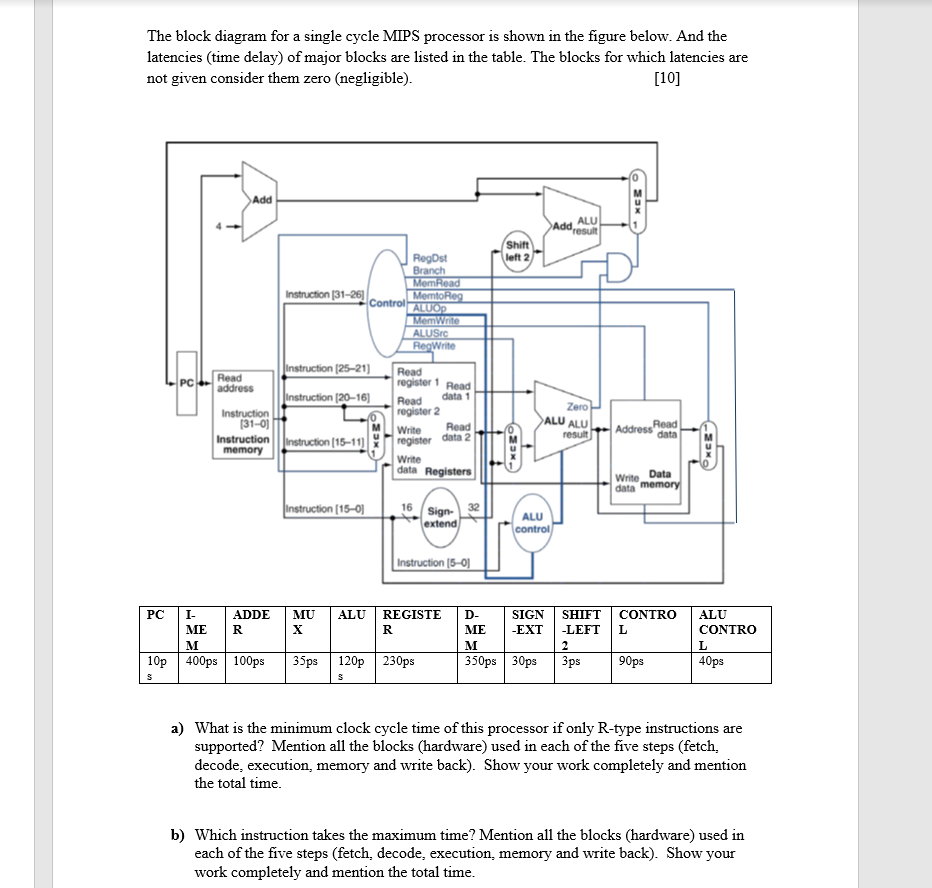
The block diagram for a single cycle MIPS processor is shown in the figure below. And the latencies (time delay) of major blocks are listed in the table. The blocks for which latencies are not given consider them zero (negligible). [10] Add Add ALU result Shift left 2 RegDst Branch MomRead Instruction (31-26] Memo Reg Control ALUOP Mem Write ALUSIC RegWrite instruction (25-21) Read Read register 1 Read address Instruction (2016) Read data 1 Instruction register 2 (31-0 Write Read Instruction instruction (15-11) memory Write data Registers Zero ALU ALU result Read Address data register data 2 Data Write data memory Instruction (15-01 16 Sign extend ALU control Instruction (5-0) ALU MU REGISTE R CONTRO L PC I- ADDE ME R M 10p 400ps 100ps D- SIGN ME -EXT M 350ps 30ps SHIFT -LEFT 2 3ps ALU CONTRO L 40ps 35ps 120p 230ps 90ps S S a) What is the minimum clock cycle time of this processor if only R-type instructions are supported? Mention all the blocks (hardware) used in each of the five steps (fetch, decode, execution memory and write back). Show your work completely and mention the total time. b) Which instruction takes the maximum time? Mention all the blocks (hardware) used in each of the five steps (fetch. decode, execution memory and write back). Show your work completely and mention the total time. The block diagram for a single cycle MIPS processor is shown in the figure below. And the latencies (time delay) of major blocks are listed in the table. The blocks for which latencies are not given consider them zero (negligible). [10] Add Add ALU result Shift left 2 RegDst Branch MomRead Instruction (31-26] Memo Reg Control ALUOP Mem Write ALUSIC RegWrite instruction (25-21) Read Read register 1 Read address Instruction (2016) Read data 1 Instruction register 2 (31-0 Write Read Instruction instruction (15-11) memory Write data Registers Zero ALU ALU result Read Address data register data 2 Data Write data memory Instruction (15-01 16 Sign extend ALU control Instruction (5-0) ALU MU REGISTE R CONTRO L PC I- ADDE ME R M 10p 400ps 100ps D- SIGN ME -EXT M 350ps 30ps SHIFT -LEFT 2 3ps ALU CONTRO L 40ps 35ps 120p 230ps 90ps S S a) What is the minimum clock cycle time of this processor if only R-type instructions are supported? Mention all the blocks (hardware) used in each of the five steps (fetch, decode, execution memory and write back). Show your work completely and mention the total time. b) Which instruction takes the maximum time? Mention all the blocks (hardware) used in each of the five steps (fetch. decode, execution memory and write back). Show your work completely and mention the total time
Step by Step Solution
There are 3 Steps involved in it

Get step-by-step solutions from verified subject matter experts