

Question: 3. Processor Cycle Time Determination Assume the following latencies for the logic blocks in Figure 4.17 from the textbook I-Mem Adder MUX ALU | Reg
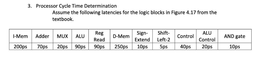
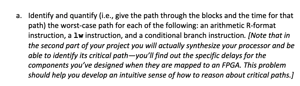
3. Processor Cycle Time Determination Assume the following latencies for the logic blocks in Figure 4.17 from the textbook I-Mem Adder MUX ALU | Reg Read D-Mem>ign-Shift- Extend Left-2 ControALU 90ps 250ps 10ps 5ps40ps 20ps 200ps 70ps 20ps 90ps Control AND 10ps a. Identify and quantify (i.e., give the path through the blocks and the time for that path) the worst-case path for each of the following: an arithmetic R-format instruction, a lw instruction, and a conditional branch instruction. [Note that in the second part of your project you will actually synthesize your processor and be able to identify its critical path-you'll find out the specific delays for the components you've designed when they are mapped to an FPGA. This problem should help you develop an intuitive sense of how to reason about critical paths. 3. Processor Cycle Time Determination Assume the following latencies for the logic blocks in Figure 4.17 from the textbook I-Mem Adder MUX ALU | Reg Read D-Mem>ign-Shift- Extend Left-2 ControALU 90ps 250ps 10ps 5ps40ps 20ps 200ps 70ps 20ps 90ps Control AND 10ps a. Identify and quantify (i.e., give the path through the blocks and the time for that path) the worst-case path for each of the following: an arithmetic R-format instruction, a lw instruction, and a conditional branch instruction. [Note that in the second part of your project you will actually synthesize your processor and be able to identify its critical path-you'll find out the specific delays for the components you've designed when they are mapped to an FPGA. This problem should help you develop an intuitive sense of how to reason about critical paths
Step by Step Solution
There are 3 Steps involved in it

Get step-by-step solutions from verified subject matter experts