

Question: (a) Determine the logic expressions to implement an address decoding circuit to realize the address map shown below. Use partial address decoding technique in your
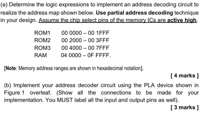
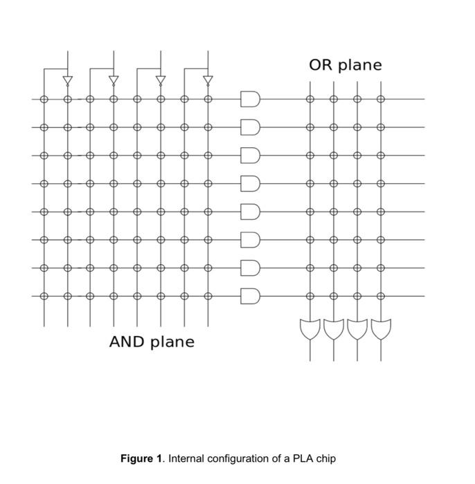
(a) Determine the logic expressions to implement an address decoding circuit to realize the address map shown below. Use partial address decoding technique in your design. Assume the chip select pins of the memory ICs are active high. ROM1 ROM2 ROM3 RAM 00 0000-00 1FFF 00 2000 - 00 3FFF 00 4000 - 00 7FFF 04 0000 - OF FFFF. [Note: Memory address ranges are shown in hexadecimal notation). [ 4 marks ] (b) Implement your address decoder circuit using the PLA device shown in Figure 1 overleaf. (Show all the connections to be made for your implementation. You MUST label all the input and output pins as well). [3 marks ] OR plane AND plane Figure 1. Internal configuration of a PLA chip
Step by Step Solution
There are 3 Steps involved in it

Get step-by-step solutions from verified subject matter experts