

Question: Circuit 1: Design a four-bit arithmetic logic unit (ALU) connected with an 8 x 9 memory. The circuit has two four-bit input data paths (AO,
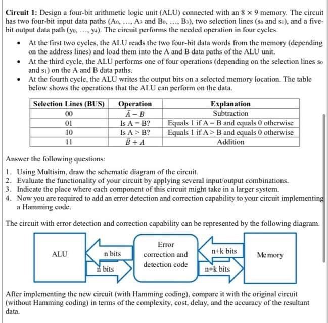
Circuit 1: Design a four-bit arithmetic logic unit (ALU) connected with an 8 x 9 memory. The circuit has two four-bit input data paths (AO, ..., Az and Bo, .... Bs), two selection lines (so and s), and a five- bit output data path (yo..... y4). The circuit performs the needed operation in four cycles. At the first two cycles, the ALU reads the two four-bit data words from the memory (depending on the address lines) and load them into the A and B data paths of the ALU unit. At the third cycle, the ALU performs one of four operations (depending on the selection lines so and si) on the A and B data paths. At the fourth cycle, the ALU writes the output bits on a selected memory location. The table below shows the operations that the ALU can perform on the data. Selection Lines (BUS) Operation Explanation 00 A-B Subtraction 01 Is A = B? Equals 1 if A= B and equals 0 otherwise 10 Is A >B? Equals 1 if A> B and cquals 0 otherwise B + A Addition Answer the following questions: 1. Using Multisim, draw the schematic diagram of the circuit. 2. Evaluate the functionality of your circuit by applying several input/output combinations. 3. Indicate the place where cach component of this circuit might take in a larger system. 4. Now you are required to add an error detection and correction capability to your circuit implementing a Hamming code. The circuit with error detection and correction capability can be represented by the following diagram. ALU Error correction and detection code n+k bits n bits bits Memory n+k bits After implementing the new circuit (with Hamming coding), compare it with the original circuit (without Hamming coding) in terms of the complexity, cost, delay, and the accuracy of the resultant data
Step by Step Solution
There are 3 Steps involved in it

Get step-by-step solutions from verified subject matter experts