

Question: Consider a p-type semiconductor being contacted by a metal to form a metal-semiconductor junction, based on the energy level diagram below. a) First consider metal
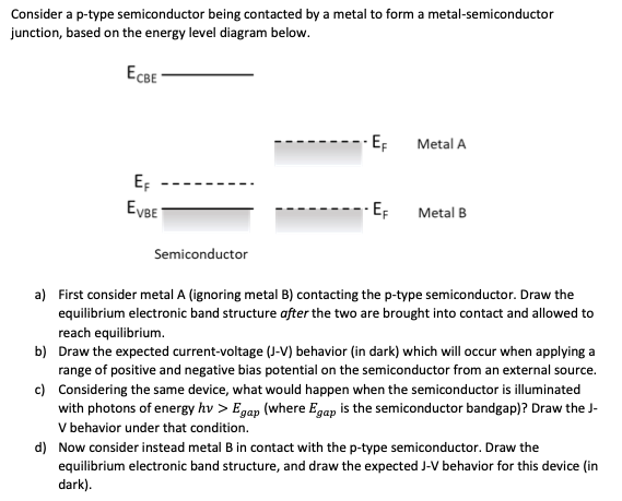
Consider a p-type semiconductor being contacted by a metal to form a metal-semiconductor junction, based on the energy level diagram below. a) First consider metal A (ignoring metal B) contacting the p-type semiconductor. Draw the equilibrium electronic band structure after the two are brought into contact and allowed to reach equilibrium. b) Draw the expected current-voltage (J-V) behavior (in dark) which will occur when applying a range of positive and negative bias potential on the semiconductor from an external source. c) Considering the same device, what would happen when the semiconductor is illuminated with photons of energy hv>Egap (where Egap is the semiconductor bandgap)? Draw the JV behavior under that condition. d) Now consider instead metal B in contact with the p-type semiconductor. Draw the equilibrium electronic band structure, and draw the expected J-V behavior for this device (in dark)
Step by Step Solution
There are 3 Steps involved in it

Get step-by-step solutions from verified subject matter experts