

Question: Design and show the schematic for a synchronous binary logic circuit that implements this state diagram. The system has two external inputs X and Y.
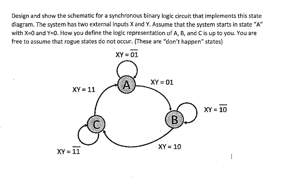
Design and show the schematic for a synchronous binary logic circuit that implements this state diagram. The system has two external inputs X and Y. Assume that the system starts in state "A" with X = 0 and Y = 0. How you define the logic representation of A, B, and C is up to you. You are free to assume that rogue states do not occur. (These are "don't happen" states) Design and show the schematic for a synchronous binary logic circuit that implements this state diagram. The system has two external inputs X and Y. Assume that the system starts in state "A" with X = 0 and Y = 0. How you define the logic representation of A, B, and C is up to you. You are free to assume that rogue states do not occur. (These are "don't happen" states)
Step by Step Solution
There are 3 Steps involved in it

Get step-by-step solutions from verified subject matter experts