

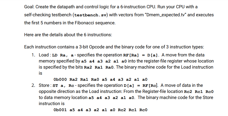
Question: Goal: Create the datapath and control logic for a 6 - instruction CPU. Run your CPU with a self - checking testbench ( testbench .
Goal: Create the datapath and control logic for a instruction CPU. Run your CPU with a
selfchecking testbench testbenchsv with vectors from "Dmemexpected.tv and executes
the first numbers in the Fibonacci sequence.
Here are the details about the instructions:
Each instruction contains a bit Opcode and the binary code for one of instruction types:
Load: LD Ra aspecifies the operation RFRa Da A move from the data
memory specified by a a a a a a into the registerfile register whose location
is specified by the bits Ra Ra Ra The binary machine code for the Load instruction
is
Ob Ra Ra Ra a a a a a a
Store:ST a Rcspecifies the operation DaRFRc A move of data in the
opposite direction as the Load instruction: From the Registerfile location Rc Rc Rc
to data memory location a a a a a a The binary machine code for the Store
instruction is
Ob a a a a a a Rc Rc Rc
where the function is performed on the data in Rb Rb Rb and Rc Rc Rc
result is stored the register specified by Ra Ra Ra The functions in XXX are AD
SUB, AND and OR:
ADD Ob Ra Ra Ra Rb Rb Rb Rc Rc Rc
SUB Ob Ra Ra Ra Rb Rb Rb Rc Rc Rc
AND Ob Ra Ra Ra Rb Rb Rb Rc Rc Rc
OR Ob Ra Ra Ra Rb Rb Rb Rc Rc Rc
The datapath will have a Proaram Counter. Instruction Memory. Data Memory. Reaister File.
ALUtype: xxXRa,RbRcSpecifies the operation RFRaFRFRbRFRc where the function is performed on the data in Rb Rb Rb and Rc Rc Rc The result is stored the register specified by Ra Ra Ra The functions in XXX are ADD, SUB, AND and OR:
ADD Ob Ra Ra Ra Rb Rb Rb Rc Rc Rc
SUB Ob Ra Ra Ra Rb Rb Rb Rc Rc Rc
AND Ob Ra Ra Ra Rb Rb Rb Rc Rc Rc
OR Ob Ra Ra Ra Rb Rb Rb Rc Rc Rc
The datapath will have a Program Counter, Instruction Memory, Data Memory, Register File, : muxes and ALU. In a singlecycle the CPU will fetch the instruction from the Instruction Memory, Read from the Memory to the Register File Load perform the ALU for ALU type instructions and write back to the Memory from the Register File Store
The CPU microarchitecture :
Part instruction CPU Control Logic
In this section, we will create the control logic for the instruction programmable processor.
Based on the bit input Instruction: Name this verilog file controller.sv
The ALUcontrol table is:
Create a testbench to test your control logic to see the outputs change for each of the following instructions: LD ST ADD, SUB, AND, OR
Include a snapshot of the EDA playground waveform showing the correct outputs for the above sequence and fill out the below table with the values in binary.
Cycle # Instruction LD ST ADD SUB AND OR RF Wwe ALUcontrol DMEM we Muxselect M Muxselect M please help me to this testbench.sv design.sv and controller.sv please
Step by Step Solution
There are 3 Steps involved in it
1 Expert Approved Answer
Step: 1 Unlock

Question Has Been Solved by an Expert!
Get step-by-step solutions from verified subject matter experts
Step: 2 Unlock
Step: 3 Unlock