

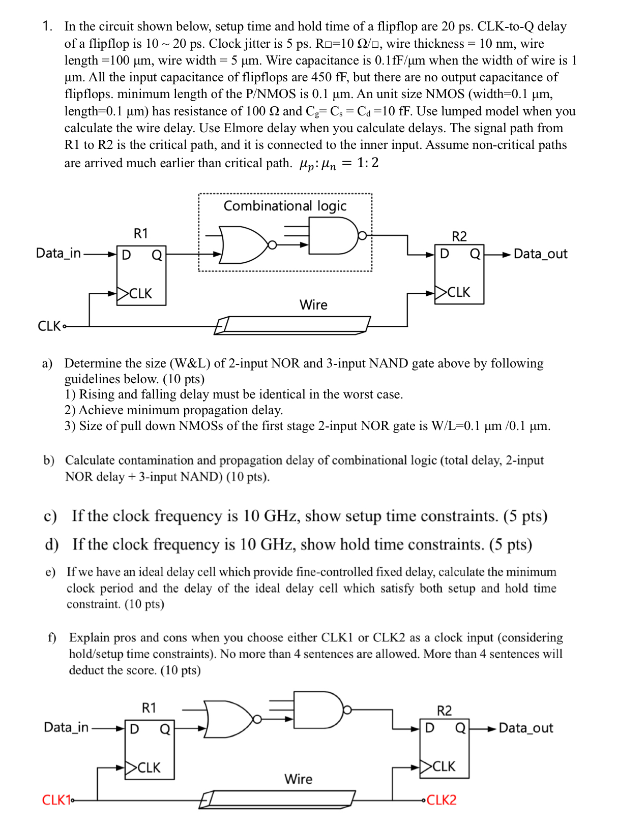
Question: In the circuit shown below, setup time and hold time of a flipflop are 2 0 ps . CLK - to - Q delay of
In the circuit shown below, setup time and hold time of a flipflop are ps CLKtoQ delay of a flipflop is Clock jitter is wire thickness wire length wire width Wire capacitance is when the width of wire is All the input capacitance of flipflops are fF but there are no output capacitance of flipflops. minimum length of the MOS is An unit size NMOS width length has resistance of and Use lumped model when you calculate the wire delay. Use Elmore delay when you calculate delays. The signal path from R to R is the critical path, and it is connected to the inner input. Assume noncritical paths are arrived much earlier than critical path. ::
a Determine the size W&L of input NOR and input NAND gate above by following guidelines below. pts
Rising and falling delay must be identical in the worst case.
Achieve minimum propagation delay.
Size of pull down NMOSs of the first stage input NOR gate is
b Calculate contamination and propagation delay of combinational logic total delay, input NOR delay input NAND pts
c If the clock frequency is GHz show setup time constraints. pts
d If the clock frequency is GHz show hold time constraints. pts
e If we have an ideal delay cell which provide finecontrolled fixed delay, calculate the minimum clock period and the delay of the ideal delay cell which satisfy both setup and hold time constraint. pts
f Explain pros and cons when you choose either CLK or CLK as a clock input considering holdsetup time constraints No more than sentences are allowed. More than sentences will deduct the score. pts
Step by Step Solution
There are 3 Steps involved in it
1 Expert Approved Answer
Step: 1 Unlock

Question Has Been Solved by an Expert!
Get step-by-step solutions from verified subject matter experts
Step: 2 Unlock
Step: 3 Unlock