

Question: include test bench and wave simulation please and thank you The BCD counter circuit has one input clk, and four-bit output signal dout. The dout
include test bench and wave simulation please and thank you
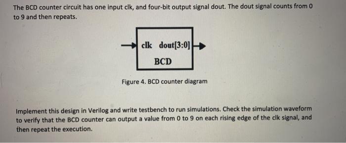
The BCD counter circuit has one input clk, and four-bit output signal dout. The dout signal counts from 0 to 9 and then repeats. clk dout[3:0] BCD Figure 4. BCD counter diagram Implement this design in Verilog and write testbench to run simulations. Check the simulation waveform to verify that the BCD counter can output a value from 0 to 9 on each rising edge of the clk signal, and then repeat the execution
Step by Step Solution
There are 3 Steps involved in it
1 Expert Approved Answer
Step: 1 Unlock

Question Has Been Solved by an Expert!
Get step-by-step solutions from verified subject matter experts
Step: 2 Unlock
Step: 3 Unlock