

Question: include wave simulation and test bench if possible The binary combinational multiplier diagram: X2 X Xo YO X Y2 Y X Yo Xo Yo X,
 include wave simulation and test bench if possible
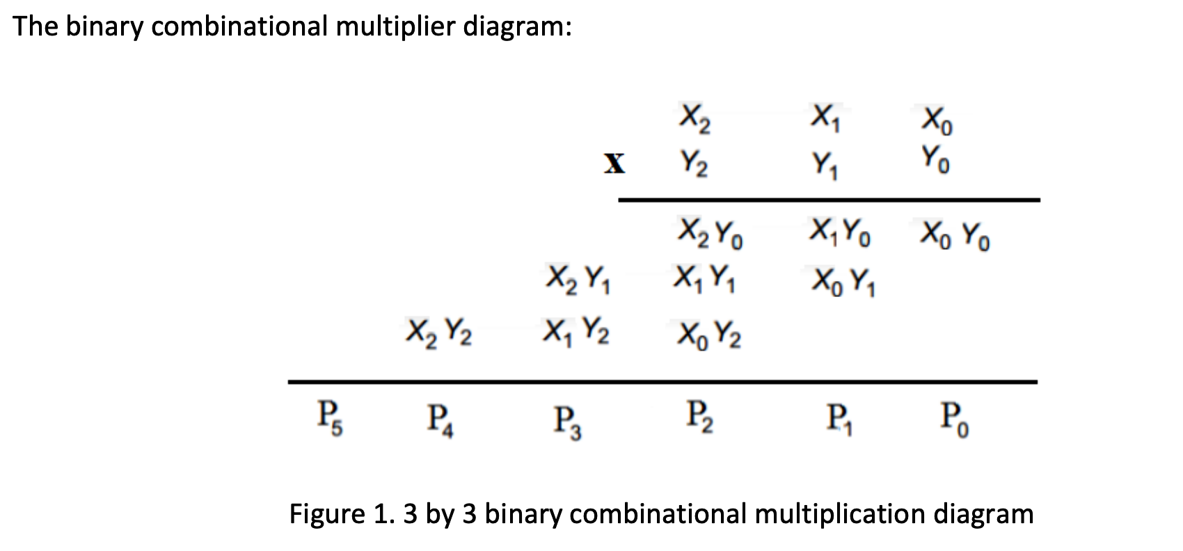
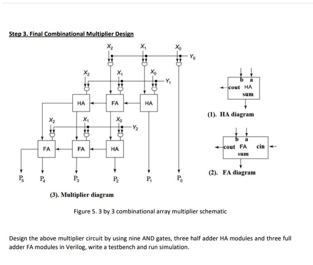
The binary combinational multiplier diagram: X2 X Xo YO X Y2 Y X Yo Xo Yo X, Yo Xo Y, X Y, X, Y2 X, Y, XoY2 X, Y, P PA . P2 P.; P. Figure 1.3 by 3 binary combinational multiplication diagram Step 3. Final Combinational Multiplier Design X X Xo Yo X X Xo Y cout HA sum HA FA HA (1). HA diagram Xo XB0 Y2 WY cin FA FA HA cout FA sum (2). FA diagram P: PA P3 P2 P, (3). Multiplier diagram Figure 5. 3 by 3 combinational array multiplier schematic Design the above multiplier circuit by using nine AND gates, three half adder HA modules and three full adder FA modules in Verilog, write a testbench and run simulation. The binary combinational multiplier diagram: X2 X Xo YO X Y2 Y X Yo Xo Yo X, Yo Xo Y, X Y, X, Y2 X, Y, XoY2 X, Y, P PA . P2 P.; P. Figure 1.3 by 3 binary combinational multiplication diagram Step 3. Final Combinational Multiplier Design X X Xo Yo X X Xo Y cout HA sum HA FA HA (1). HA diagram Xo XB0 Y2 WY cin FA FA HA cout FA sum (2). FA diagram P: PA P3 P2 P, (3). Multiplier diagram Figure 5. 3 by 3 combinational array multiplier schematic Design the above multiplier circuit by using nine AND gates, three half adder HA modules and three full adder FA modules in Verilog, write a testbench and run simulation
Step by Step Solution
There are 3 Steps involved in it

Get step-by-step solutions from verified subject matter experts