

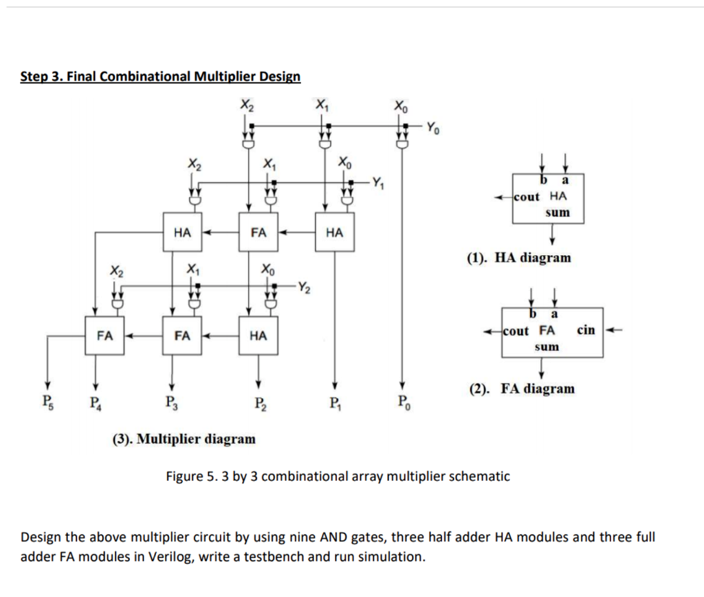
Question: Verilog code, if possible show wave simulation as well Step 3. Final Combinational Multiplier Design X X Xo Yo X X Xo Y cout HA
Verilog code, if possible show wave simulation as well
Step 3. Final Combinational Multiplier Design X X Xo Yo X X Xo Y cout HA sum HA FA HA (1). HA diagram Xo XB0 Y2 WY cin FA FA HA cout FA sum (2). FA diagram P: PA P3 P2 P, (3). Multiplier diagram Figure 5. 3 by 3 combinational array multiplier schematic Design the above multiplier circuit by using nine AND gates, three half adder HA modules and three full adder FA modules in Verilog, write a testbench and run simulation
Step by Step Solution
There are 3 Steps involved in it
1 Expert Approved Answer
Step: 1 Unlock

Question Has Been Solved by an Expert!
Get step-by-step solutions from verified subject matter experts
Step: 2 Unlock
Step: 3 Unlock