

Question: NO.2 HARDWARE PROTOTYPING USING ALTERA DE2-70 1) In this task, you will be using the ALTERA DE2-70 board, set the device number as EP2 C70F896C6.
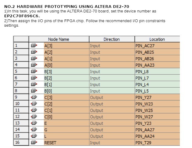
NO.2 HARDWARE PROTOTYPING USING ALTERA DE2-70 1) In this task, you will be using the ALTERA DE2-70 board, set the device number as EP2 C70F896C6. 2)Then assign the I/O pins of the FPGA chip. Follow the recommended I/O pin constraints settings. Node Name Direction Location A[3] Input PIN_AC27 2 A[2] Input PIN AB25 3 A[1] Input PIN AB26 4 A[0] Input PIN AA23 5 B[3] Input PIN L8 6 B[2] Input PIN L7 7 B[1] Input PIN L4 B[0] Input PIN L5 C[3] Output PIN_Y27 10 C[2] Output PIN_W23 11 C[1] Output PIN_W25 12 C Output PIN W27 13 E Output PIN Y23 14 G Output PIN AA27 15 L Output PIN AA24 16 RESET Input PIN T29
Step by Step Solution
There are 3 Steps involved in it
1 Expert Approved Answer
Step: 1 Unlock

Question Has Been Solved by an Expert!
Get step-by-step solutions from verified subject matter experts
Step: 2 Unlock
Step: 3 Unlock