

Question: PC+1+ se k or k16 PC+1 Fetch Program Memory Inst Data Out k16 PC+1 SP+1 or SP-1 AR, AR+1 AR-1, or AR+q PC+1 IR DMAR
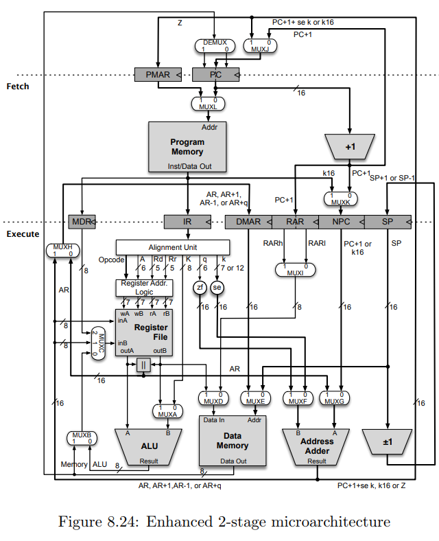
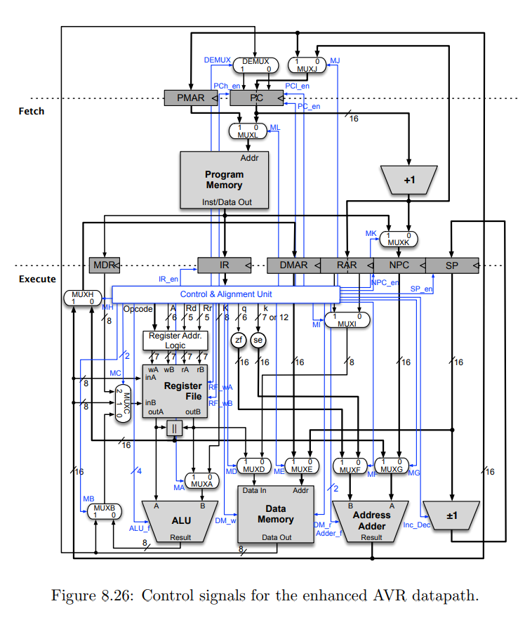
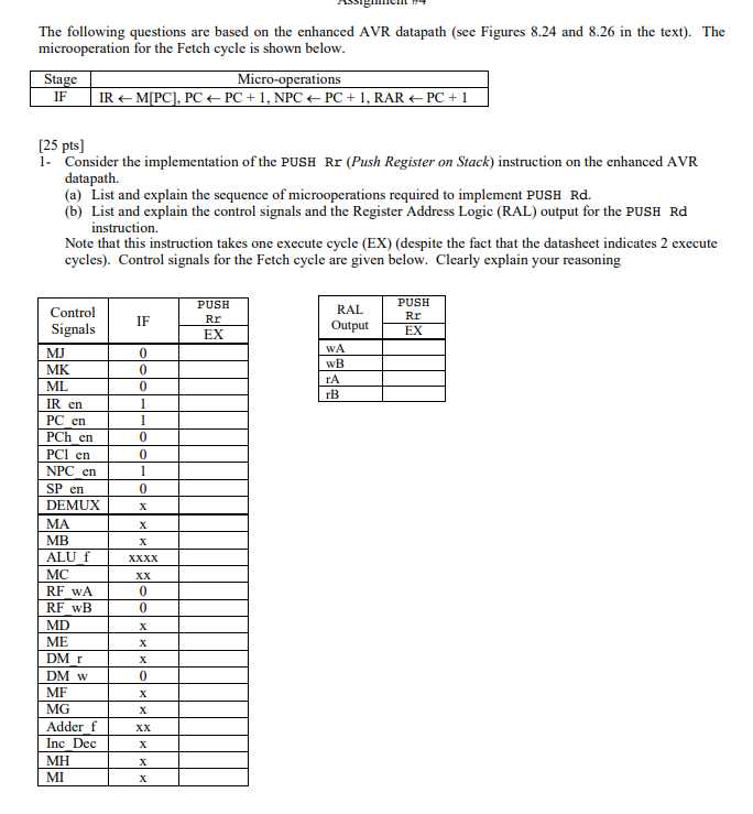
PC+1+ se k or k16 PC+1 Fetch Program Memory Inst Data Out k16 PC+1 SP+1 or SP-1 AR, AR+1 AR-1, or AR+q PC+1 IR DMAR NPC Execute RARI PC+1 or k16 SP Alignment Unit zf (se AR Register File outB AR MUXE Data In Data Memory Address Adder ALU Result Data Out Memory ALU 8 AR, AR+1,AR-1, or AR+q PC+1+se k, k16 or Z Figure 8.24: Enhanced 2-stage microarchitecture DEMUX MJ PCh en PCI en en Fetch ML Addr Program Memory Inst/Data Out MK IR DMAR NPC SP Execute R en PC e SP Control & Alignment Unit 6 /70 12 ister Addr zf (se 16 16 Register File inB Data In MB Data Memory AddresS ALU DM w Adder Inc Result ALU Result Data Out Figure 8.26: Control signals for the enhanced AVR datapath. The following questions are based on the enhanced AVR datapath (see Figures 8.24 and 8.26 in the text). The microoperation for the Fetch cycle is shown below Sta IF erations 25 pts] Consider the implementation of the PUSH Rr (Push Register on Stack) instruction on the enhanced AVR datapath. (a) List and explain the sequence of microoperations required to implement PUSH Rd. (b) List and explain the control signals and the Register Address Logic (RAL) output for the PUSH Rd instruction. Note that this instruction takes one execute cycle (EX) (despite the fact that the datasheet indicates 2 execute cycles). Control signals for the Fetch cycle are given below. Clearly explain your reasoning Control Signals PUSH Rr EX RAL PUSH OutputEX Rr IF WA MK ML TA cn PC en PCh en PCI en NPC en cn DEMUX MA MB ALU MC RF wA RF wB ME DM r DM w MF MG Adder f Inc Dec MI PC+1+ se k or k16 PC+1 Fetch Program Memory Inst Data Out k16 PC+1 SP+1 or SP-1 AR, AR+1 AR-1, or AR+q PC+1 IR DMAR NPC Execute RARI PC+1 or k16 SP Alignment Unit zf (se AR Register File outB AR MUXE Data In Data Memory Address Adder ALU Result Data Out Memory ALU 8 AR, AR+1,AR-1, or AR+q PC+1+se k, k16 or Z Figure 8.24: Enhanced 2-stage microarchitecture DEMUX MJ PCh en PCI en en Fetch ML Addr Program Memory Inst/Data Out MK IR DMAR NPC SP Execute R en PC e SP Control & Alignment Unit 6 /70 12 ister Addr zf (se 16 16 Register File inB Data In MB Data Memory AddresS ALU DM w Adder Inc Result ALU Result Data Out Figure 8.26: Control signals for the enhanced AVR datapath. The following questions are based on the enhanced AVR datapath (see Figures 8.24 and 8.26 in the text). The microoperation for the Fetch cycle is shown below Sta IF erations 25 pts] Consider the implementation of the PUSH Rr (Push Register on Stack) instruction on the enhanced AVR datapath. (a) List and explain the sequence of microoperations required to implement PUSH Rd. (b) List and explain the control signals and the Register Address Logic (RAL) output for the PUSH Rd instruction. Note that this instruction takes one execute cycle (EX) (despite the fact that the datasheet indicates 2 execute cycles). Control signals for the Fetch cycle are given below. Clearly explain your reasoning Control Signals PUSH Rr EX RAL PUSH OutputEX Rr IF WA MK ML TA cn PC en PCh en PCI en NPC en cn DEMUX MA MB ALU MC RF wA RF wB ME DM r DM w MF MG Adder f Inc Dec MI
Step by Step Solution
There are 3 Steps involved in it

Get step-by-step solutions from verified subject matter experts