

Question: Please draw all 4 circuits. Please try using Logisim or you can just draw. 1) SR Latch (Using NOR Gates) Design a circuit (called SR_GATES)
Please draw all 4 circuits. Please try using Logisim or you can just draw.
1)
SR Latch (Using NOR Gates)
Design a circuit (called SR_GATES) that takes two inputs (S, for set, and R, for reset) and produces two outputs (Q, the value latched, and NOT_Q, the inverse of Q). The circuit will implement the following SR latch:
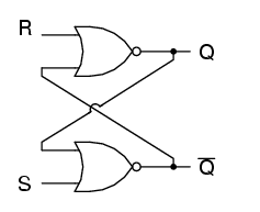
This circuit will have the following behaviour:
| R | S | Q | NOT_Q |
| 0 | 0 | no change | no change |
| 0 | 1 | 1 | 0 |
| 1 | 0 | 0 | 1 |
| 1 | 1 | undefined | undefined |
2)
SR Latch (Using the 7402 Logic Chip)
For this circuit (called SR_LATCH), rather than use the gates themselves, you will build using a 7402 logic chip (which contains 4 NOR gates). If you look in the TTL section of the top-left panel, you will find a chip called a 7402 (quad 2-input NOR gate). Drag this into your circuit. Click the chip and set 'ShowInternalStructure' to True in the properties panel, so that you can see the gates inside the chip. Using these gates, create the exact same circuit as in the previous component.
3)
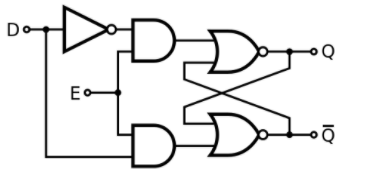
D Flip Flop (Using Your SR_LATCH Circuit and AND Gates)
Design a circuit (called DFF_GATES) which has two inputs (D, the data input, and E, the enable input). When E is set high (i.e. set to 1), the value of the D input is latched by an SR latch (using your SR_LATCH component). The circuit diagram for the entire circuit is given below, but the two NOR gates on the right side are already included in your SR_LATCH circuit. Add an SR_LATCH component, then add the remaining gates, inputs, and outputs to complete the circuit.
4)
D Flip Flop (Using the 7400 Logic Chip)
For this circuit (called DFF), rather than use the gates themselves, you will build a D flip flop using only 7400 logic chips (which contains 4 NAND gates). The inputs, outputs, and behaviour should be identical to the D flip flop defined above (DFF_GATES).
If you look in the TTL section of the top-left panel, you will find a chip called a 7400 (quad 2-input NAND gate). Drag this into your circuit. Click the chip and set 'ShowInternalStructure' to True in the properties panel, so that you can see the gates inside the chip. Using these logic chips, create the exact same circuit as in the previous component. The diagram for this component with NAND gates is given below:
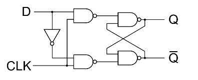
Note: You can make a NOT gate by feeding the D value into both inputs of a NAND gate.
R Q Q S A E- D OI D Q IS IO CLK
Step by Step Solution
There are 3 Steps involved in it

Get step-by-step solutions from verified subject matter experts