

Question: PRELIMINARY WORK: Consider a typical CMOS inverter for V D D = 5 V and the transistor parameters are V T n = - V
PRELIMINARY WORK:
Consider a typical CMOS inverter for and the transistor parameters are and Answer the following questions accordingly.
a Determine and plot the Voltage Transfer Characteristics VTC of Vs for the typical CMOS inverter.
b Determine the critical input and output voltages ie and You can find out from the simulation
c Determine low and high noise margins. ie and
d Explain the effects of and on and from the simulation
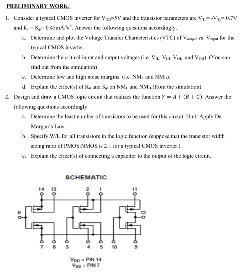
Design and draw a CMOS logic circuit that realizes the function Answer the following questions accordingly.
a Determine the least number of transistors to be used for this circuit. Hint: Apply De Morgan's Law.
b Specify WL for all transistors in the logic function suppose that the transistor width sizing ratio of PMOS:NMOS is : for a typical CMOS inverter.
c Explain the effects of connecting a capacitor to the output of the logic circuit.
Step by Step Solution
There are 3 Steps involved in it
1 Expert Approved Answer
Step: 1 Unlock

Question Has Been Solved by an Expert!
Get step-by-step solutions from verified subject matter experts
Step: 2 Unlock
Step: 3 Unlock