

Question: Project 1: Schematic Capture and VHDL Reference: Section 2.9 and 2.10 and Appendix B, Brown and Vranesic, Fundamentals of Digital Logic with VHDL Design, McGraw-Hill.
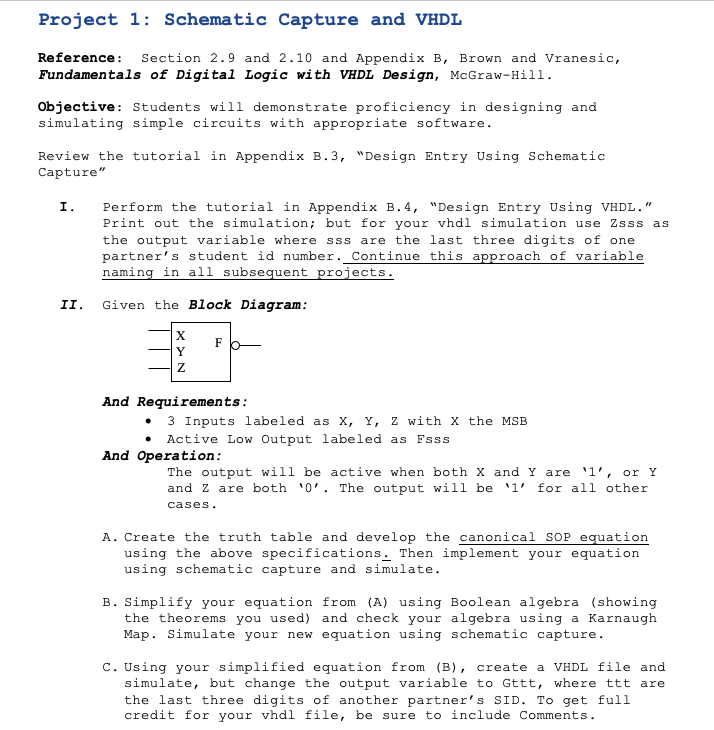
Project 1: Schematic Capture and VHDL Reference: Section 2.9 and 2.10 and Appendix B, Brown and Vranesic, Fundamentals of Digital Logic with VHDL Design, McGraw-Hill. Objective: Students will demonstrate proficiency in designing and simulating simple circuits with appropriate software. Review the tutorial in Appendix B.3, "Design Entry Using Schematic Capture" I. Perform the tutorial in Appendix B.4, "Design Entry Using VHDL." Print out the simulation; but for your vhdl simulation use Zsss as the output variable where sss are the last three digits of one partner's student id number. Continue this approach of variable naming in all subsequent projects. II. Given the Block Diagram: Fo X Y Z And Requirements: 3 Inputs labeled as X, Y, Z with x the MSB Active Low Output labeled as Fsss And Operation: The output will be active when both X and Y are '1', or y and Z are both '0'. The output will be 'l' for all other cases. A. Create the truth table and develop the canonical SOP equation using the above specifications. Then implement your equation using schematic capture and simulate. B. Simplify your equation from (A) using Boolean algebra (showing the theorems you used) and check your algebra using a Karnaugh Map. Simulate your new equation using schematic capture. C. Using your simplified equation from (B), create a VHDL file and simulate, but change the output variable to Gttt, where ttt are the last three digits of another partner's SID. To get full credit for your vhdl file, be sure to include Comments. Project 1: Schematic Capture and VHDL Reference: Section 2.9 and 2.10 and Appendix B, Brown and Vranesic, Fundamentals of Digital Logic with VHDL Design, McGraw-Hill. Objective: Students will demonstrate proficiency in designing and simulating simple circuits with appropriate software. Review the tutorial in Appendix B.3, "Design Entry Using Schematic Capture" I. Perform the tutorial in Appendix B.4, "Design Entry Using VHDL." Print out the simulation; but for your vhdl simulation use Zsss as the output variable where sss are the last three digits of one partner's student id number. Continue this approach of variable naming in all subsequent projects. II. Given the Block Diagram: Fo X Y Z And Requirements: 3 Inputs labeled as X, Y, Z with x the MSB Active Low Output labeled as Fsss And Operation: The output will be active when both X and Y are '1', or y and Z are both '0'. The output will be 'l' for all other cases. A. Create the truth table and develop the canonical SOP equation using the above specifications. Then implement your equation using schematic capture and simulate. B. Simplify your equation from (A) using Boolean algebra (showing the theorems you used) and check your algebra using a Karnaugh Map. Simulate your new equation using schematic capture. C. Using your simplified equation from (B), create a VHDL file and simulate, but change the output variable to Gttt, where ttt are the last three digits of another partner's SID. To get full credit for your vhdl file, be sure to include Comments
Step by Step Solution
There are 3 Steps involved in it

Get step-by-step solutions from verified subject matter experts