

Question: You are given the following circuit where each inverter is a sized version of the baseline inverter. a) Consider that the sizing has already
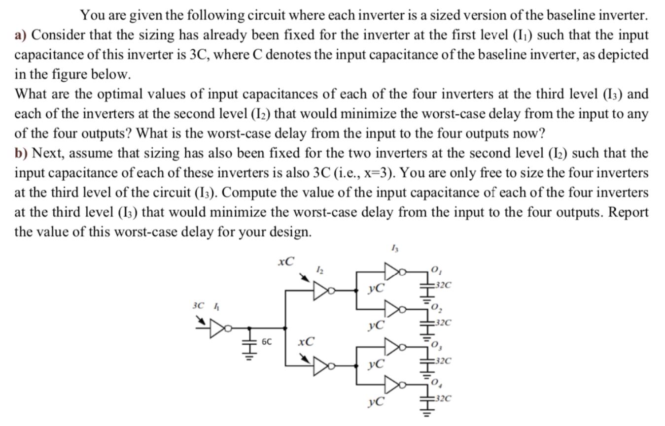
You are given the following circuit where each inverter is a sized version of the baseline inverter. a) Consider that the sizing has already been fixed for the inverter at the first level () such that the input capacitance of this inverter is 3C, where C denotes the input capacitance of the baseline inverter, as depicted in the figure below. What are the optimal values of input capacitances of each of the four inverters at the third level (13) and each of the inverters at the second level (12) that would minimize the worst-case delay from the input to any of the four outputs? What is the worst-case delay from the input to the four outputs now? b) Next, assume that sizing has also been fixed for the two inverters at the second level (12) such that the input capacitance of each of these inverters is also 3C (i.e., x=3). You are only free to size the four inverters at the third level of the circuit (13). Compute the value of the input capacitance of each of the four inverters at the third level (13) that would minimize the worst-case delay from the input to the four outputs. Report the value of this worst-case delay for your design. 3C h HH" 6C xC xC 1 yC yC YC yC 13 0 HHAHAHAH" :32C :32C 03 :32C
Step by Step Solution
3.37 Rating (156 Votes )
There are 3 Steps involved in it

Get step-by-step solutions from verified subject matter experts