

Question: The design for a full-adder shown in the figure below is used in the implementation of an 8-bit ripple carry adder in a processor
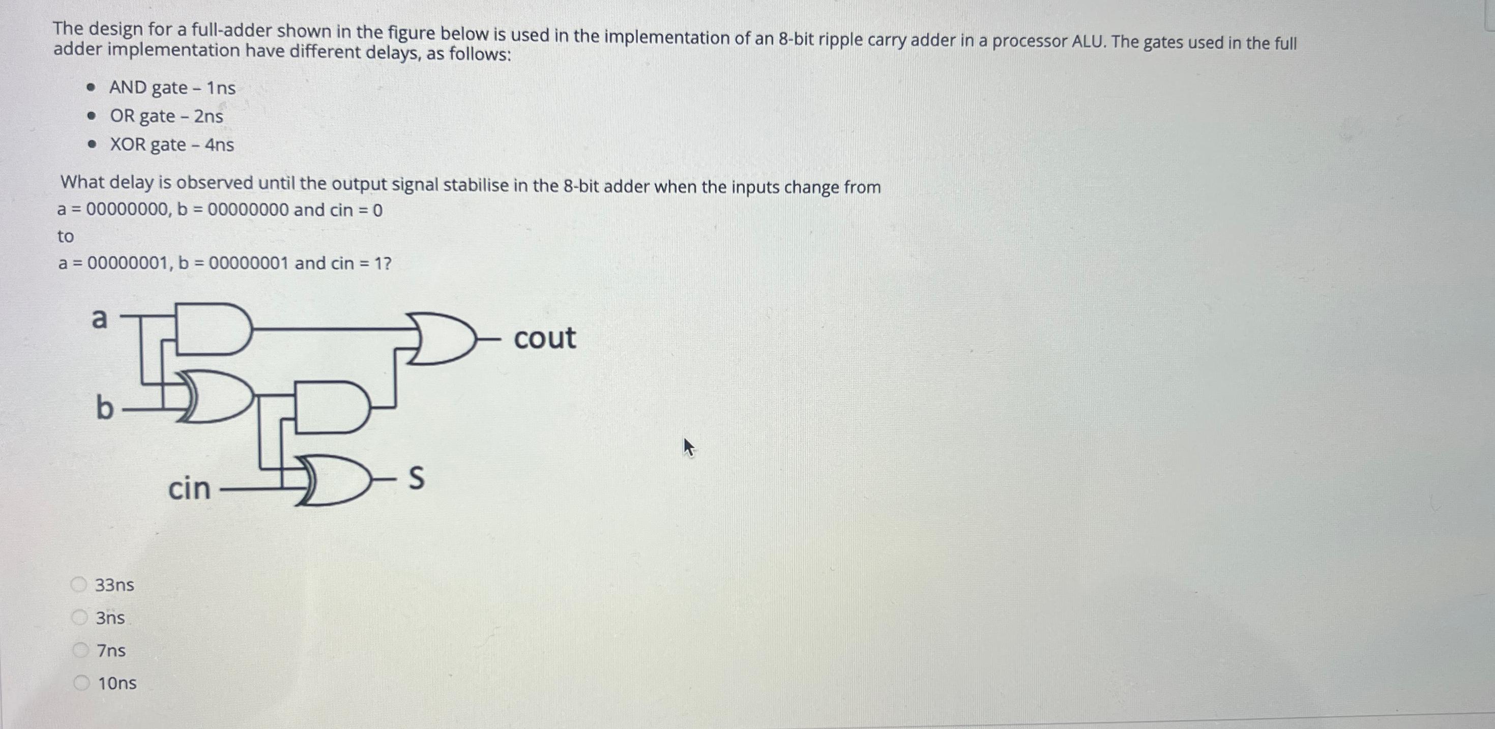
The design for a full-adder shown in the figure below is used in the implementation of an 8-bit ripple carry adder in a processor ALU. The gates used in the full adder implementation have different delays, as follows: AND gate - 1ns OR gate - 2ns XOR gate - 4ns What delay is observed until the output signal stabilise in the 8-bit adder when the inputs change from a = 00000000, b = 00000000 and cin = 0 to a = 00000001, b = 00000001 and cin = 1? a 33ns 3ns 7ns 10ns cin- D cout
Step by Step Solution
3.40 Rating (156 Votes )
There are 3 Steps involved in it
SOLUTION To determine the delay until the output signal stabilizes in the 8bit adder we need t... View full answer

Get step-by-step solutions from verified subject matter experts