

Question: this is the question.. Its from digital design.. The data flow graph (DFG) given in Figure Q5 shows the operations and data dependencies of a
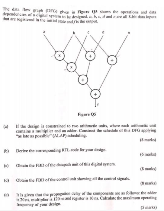
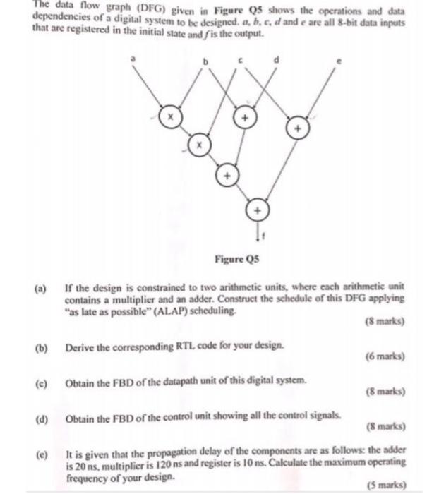
The data flow graph (DFG) given in Figure Q5 shows the operations and data dependencies of a digital system to be designed, a, b, c, d and e are all 8-bit data inputs that are registered in the initial state and fis the output. Figure 25 (a) If the design is constrained to two arithmetic units, where cach arithmetic unit contains a multiplier and an adder. Construct the schedule of this DFG applying "as late as possible" (ALAP) scheduling. (8 marks) (b) Derive the corresponding RTL code for your design. (6 marks) (c) Obtain the FBD of the datapath unit of this digital system. (8 marks) (d) Obtain the FBD of the control unit showing all the control signals. (8 marks) (e) It is given that the propagation delay of the components are as follows: the adder is 20 ns, multiplier is 120 ns and register is 10 ns. Calculate the maximum operating frequency of your design. (5 marks) The data flow graph (DFG) given in Figure 5 shows the operations and data dependencies of a digital system to be designed, a, b, c, d and e are all 8-bit data inputs that are registered in the initial state and fis the output. Figure Q5 @ (a) If the design is constrained to two arithmetic units, where each arithmetic unit contains a multiplier and an adder. Construct the schedule of this DFG applying "as late as possible" (ALAP) scheduling. (8 marks) (b) Derive the corresponding RTL code for your design. (6 marks) (c) Obtain the FBD of the datapath unit of this digital system (8 marks) (d) Obtain the FBD of the control unit showing all the control signals. (8 marks) It is given that the propagation delay of the components are as follows the adder is 20 ns, multiplier is 120 ns and register is 10 ns. Calculate the maximum operating frequency of your design. (5 marks) d The data flow graph (DFG) given in Figure Q5 shows the operations and data dependencies of a digital system to be designed, a, b, c, d and e are all 8-bit data inputs that are registered in the initial state and fis the output. Figure 25 (a) If the design is constrained to two arithmetic units, where cach arithmetic unit contains a multiplier and an adder. Construct the schedule of this DFG applying "as late as possible" (ALAP) scheduling. (8 marks) (b) Derive the corresponding RTL code for your design. (6 marks) (c) Obtain the FBD of the datapath unit of this digital system. (8 marks) (d) Obtain the FBD of the control unit showing all the control signals. (8 marks) (e) It is given that the propagation delay of the components are as follows: the adder is 20 ns, multiplier is 120 ns and register is 10 ns. Calculate the maximum operating frequency of your design. (5 marks) The data flow graph (DFG) given in Figure 5 shows the operations and data dependencies of a digital system to be designed, a, b, c, d and e are all 8-bit data inputs that are registered in the initial state and fis the output. Figure Q5 @ (a) If the design is constrained to two arithmetic units, where each arithmetic unit contains a multiplier and an adder. Construct the schedule of this DFG applying "as late as possible" (ALAP) scheduling. (8 marks) (b) Derive the corresponding RTL code for your design. (6 marks) (c) Obtain the FBD of the datapath unit of this digital system (8 marks) (d) Obtain the FBD of the control unit showing all the control signals. (8 marks) It is given that the propagation delay of the components are as follows the adder is 20 ns, multiplier is 120 ns and register is 10 ns. Calculate the maximum operating frequency of your design. (5 marks) d
Step by Step Solution
There are 3 Steps involved in it

Get step-by-step solutions from verified subject matter experts