

Question: Top Level Data bus Data Shift register input Counter Address Memory FSM Control bus Clock Figure 2: block diagram for the design Part 1: (20pts)
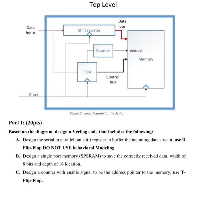
Top Level Data bus Data Shift register input Counter Address Memory FSM Control bus Clock Figure 2: block diagram for the design Part 1: (20pts) Based on the diagram, design a Verilog code that includes the following: A. Design the serial in parallel out shift register to buffer the incoming data stream, use D Flip-Flop DO NOT USE behavioral Modeling. B. Design a single port memory (SPSRAM) to save the correctly received data, width of 8 bits and depth of 16 location. C. Design a counter with enable signal to be the address pointer to the memory, use T- Flip-Flop
Step by Step Solution
There are 3 Steps involved in it
1 Expert Approved Answer
Step: 1 Unlock

Question Has Been Solved by an Expert!
Get step-by-step solutions from verified subject matter experts
Step: 2 Unlock
Step: 3 Unlock