

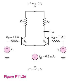
Consider a BJT diff-amp with the configuration in Figure P11.26. The signal sources have nonzero source resistances
Question:
Consider a BJT diff-amp with the configuration in Figure P11.26. The signal sources have nonzero source resistances as shown. The transistor parameters are: \(\beta=150, V_{B E}\) (on) \(=0.7 \mathrm{~V}\), and \(V_{A}=\infty\). The range of the common-mode input voltage is to be \(-3 \leq v_{C M} \leq 3 \mathrm{~V}\) and the CMRR is to be \(75 \mathrm{~dB}\).
(a) Design the diff-amp to produce the maximum possible differential-mode voltage gain.
(b) Design the current source to produce the desired bias current and CMRR.
Fantastic news! We've Found the answer you've been seeking!
Step by Step Answer:

Answered By
Asish Chandran
Other than the teaching experience that I have acquired during my masters in Electrical and Electronics Engineering, I am having 2 year of teaching experience at Indian Institute of Technology Palakkad which is one of the reputed Engineering college in India. Also I was working as a part time tutor during my bachelor degree days.
0 Reviews
10+ Question Solved
Related Book For 

Microelectronics Circuit Analysis And Design
ISBN: 9780071289474
4th Edition
Authors: Donald A. Neamen
Question Posted:
