

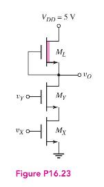
Question: Consider a four-input NMOS NAND logic gate with a depletion load similar to the circuit in Figure P16.23. The bias voltage is (V_{D D}=3.3 mathrm{~V}),
Consider a four-input NMOS NAND logic gate with a depletion load similar to the circuit in Figure P16.23. The bias voltage is \(V_{D D}=3.3 \mathrm{~V}\), and the threshold voltages are \(V_{T N D}=0.4 \mathrm{~V}\) and \(V_{T N L}=-0.6 \mathrm{~V}\). The logic 0 output voltage is to be \(0.10 \mathrm{~V}\).
(a) Using approximation methods, determine \(K_{D} / K_{L}\).
(b) The maximum power dissipation in the circuit is to be \(100 \mu \mathrm{W}\). Determine \((W / L)_{L}\) and \((W / L)_{D}\).
UX Ly Figure P16.23 VDD=5V ML My -010 My
Step by Step Solution
★★★★★
3.28 Rating (148 Votes )
There are 3 Steps involved in it
1 Expert Approved Answer
Step: 1 Unlock

Question Has Been Solved by an Expert!
Get step-by-step solutions from verified subject matter experts
Step: 2 Unlock
Step: 3 Unlock