

Question: Repeat Problem 16.44 if the circuit and transistor parameters are (V_{D D}=2.5 mathrm{~V}), (V_{T N}=0.35 mathrm{~V}, V_{T P}=-0.35 mathrm{~V}, K_{n}=100 mu mathrm{A} / mathrm{V}^{2}), and
Repeat Problem 16.44 if the circuit and transistor parameters are \(V_{D D}=2.5 \mathrm{~V}\), \(V_{T N}=0.35 \mathrm{~V}, V_{T P}=-0.35 \mathrm{~V}, K_{n}=100 \mu \mathrm{A} / \mathrm{V}^{2}\), and \(K_{p}=50 \mu \mathrm{A} / \mathrm{V}^{2}\).
Data From Problem 16.44:-
The CMOS inverter in Figure 16.21 is biased at \(V_{D D}=3.3 \mathrm{~V}\). Let \(K_{n}=K_{p}\), \(V_{T N}=0.5 \mathrm{~V}\), and \(V_{T P}=-0.5 \mathrm{~V}\).
(a) Determine the two values of \(v_{I}\) and the corresponding values of \(v_{O}\) for which \(\left(d v_{O} / d v_{I}\right)=-1\) on the voltage transfer characteristics.
(b) Find the noise margins.
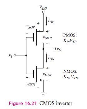
USGP + VDD iDP + PMOS: USDP Kp,VTP + iDN NMOS: UDSN + KN, VTN VGSN Figure 16.21 CMOS inverter
Step by Step Solution
3.31 Rating (157 Votes )
There are 3 Steps involved in it

Get step-by-step solutions from verified subject matter experts