

Question: Aband-gap reference circuit is shown in Fig. 4.63. Assume that β F , VA, I S1 = 1 à 10 15 A, and I S2
Aband-gap reference circuit is shown in Fig. 4.63. Assume that βF†’ ˆž, VA†’ˆž, IS1= 1 × 10ˆ’15A, and IS2= 8 × 10ˆ’15A. Assume the op amp is ideal except for a possibly nonzero offset voltage VOS, which is modeled by a voltage source in Fig. 4.63.
(a) Suppose that R2 is trimmed to set VOUT equal to the target voltage for which dVOUT/dT = 0 at T = 25 °C when VOS = 0. Find dVOUT/dT at T = 25 °C when VOS = 30 mV.
(b) Under the conditions in part (a), is dVOUT/dT positive or negative? Explain.
Fig. 4.63:
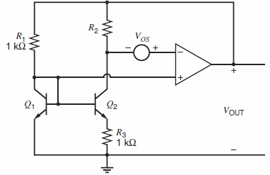
R2 Vos R1 1 k Q2 VOUT R3 1 k2
Step by Step Solution
3.46 Rating (153 Votes )
There are 3 Steps involved in it
a Negative feedback forces V C2 V BE1 V OS V OUT ... View full answer

Get step-by-step solutions from verified subject matter experts
Document Format (2 attachments)
1528_605d88e1b015d_686844.pdf
180 KBs PDF File
1528_605d88e1b015d_686844.docx
120 KBs Word File