

Question: Repeat Problem 9.23, but skip the SPICE simulation. Here, M 9 will be used in the op amp in Fig. 6.58. Let V DD =
Table 2.4:
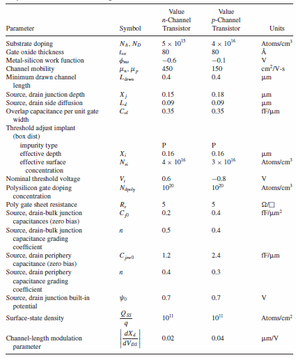
Value Value -Channel p-Channel Parameter Symbol Transistor Transistor Units NA. ND 5 x 10⁵ Substrate doping 4 x 10¹⁶ Atoms/cm Gate oxide thickness 80 80 Metal-silicon work function -0.6 -0.1 cm?/V-s Channel mobility 450 150 Minimum drawn channel Len 0.4 0.4 length Source, drain junction depth Source, drain side diffusion Overlap capacitance per unit gate width Threshold adjust implant (box dist) , La Cal 0.15 0.18 0.09 0.09 0.35 0.35 T/m impurity type effective depth X; 0.16 0.16 3 x 10¹⁶ Atoms/cm effective surface 4 x 10¹⁶ concentration Nominal threshold voltage V, Napeiy -0.8 10 0.6 10 Polysilicon gate doping Atoms/cm concentration R, Cp Poly gate sheet resistance Source, drain-bulk junction capacitances (zero bias) Source, drain-bulk junction capacitance grading F/um? 0.2 0.4 0.5 0.4 coefficient C ja Source, drain periphery capacitance (zero bias) Source, drain periphery capacitance grading 1.2 2.4 T/m 0.4 0.3 coefficient Source, drain junction built-in potential 0.7 0.7 Oss Surface-state density 10! 10" Atoms/cm? dX4 Channel-length modulation 0.02 0.04 /V dVos parameter
Step by Step Solution
3.34 Rating (154 Votes )
There are 3 Steps involved in it
From problem 922 1R 9 k WL 9 V GS9 V t9 Since I D12 I D6 and WL 12 WL 6 ... View full answer

Get step-by-step solutions from verified subject matter experts
Document Format (2 attachments)
1528_605d88e1c7629_687095.pdf
180 KBs PDF File
1528_605d88e1c7629_687095.docx
120 KBs Word File