

Question: Two flip-flops are connected as shown in the following diagram. The delay represents wiring delay between the two clock inputs, which results in clock skew.
Two flip-flops are connected as shown in the following diagram. The delay represents wiring delay between the two clock inputs, which results in clock skew. This can cause possible loss of synchronization. The flip-flop propagation delay from clock to Q is 10 ns < tp< 15 ns, and the setup and hold times for D1are always satisfied.
(a) What is the maximum value that the delay can have and still achieve proper synchronous operation? Draw a timing diagram to justify your answer.
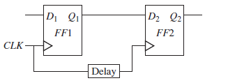
(b) Assuming that the delay is ,3 ns, what is the minimum allowable clock period?
D2 Q2 DI Qi FF1 FF2 CLK- Delay
Step by Step Solution
★★★★★
3.42 Rating (171 Votes )
There are 3 Steps involved in it
1 Expert Approved Answer
Step: 1 Unlock

a delay t pmin t h 102 8 ... View full answer
Question Has Been Solved by an Expert!
Get step-by-step solutions from verified subject matter experts
Step: 2 Unlock
Step: 3 Unlock