

Question: Using Figure 3-31 as a guide, write a structural Verilog description for the fulladder circuit in Figure 3-58. Compile and simulate your description. Apply all
Using Figure 3-31 as a guide, write a structural Verilog description for the fulladder circuit in Figure 3-58. Compile and simulate your description. Apply all eight input combinations to check the correction function of your description.
Figure 3-31
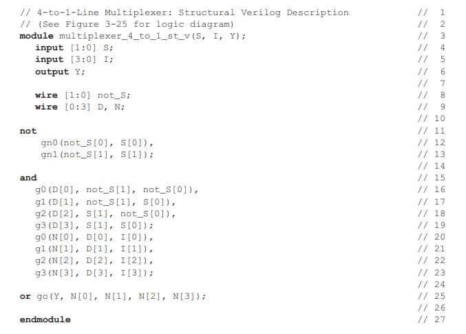
Figure 3-58
// 4-to-1-Line Multiplexer: Structural Verilog Description // (See Figure 3-25 for logic diagram) module multiplexer_4_to_1_st_v (S, I, Y); input [1:0] S; input [3:0] I; output Y; wire [1:0] not_S; wire [0:3] D, N; not and gno (not_S[0], s[0]), gn1 (not_S [1], S[1]); g0 (D [0], not_S [1], gl (D[1], not_s [1], s[0]), g2 (D[2], S[11], not_S[0]), g3 (D[3], S[1], S[0]); g0 (N[0], D[0], I[0]), g1 (N[1], D[1], I[1]), g2 (N[2], D[2], I[2]), g3 (N[3], D[3], I [3]); or go (Y, N[0], N[1], N[2], N[3]); not_S[0]), endmodule // // // 11 // 1234 o 5 7 // // 9 // 10 // 11 // 12 // 13 // 14 // 15 // 16 // 17 // 18 // 19 // 20 // 21 // 22 // 23 // 24 // 25 // 26 // 27
Step by Step Solution
3.40 Rating (162 Votes )
There are 3 Steps involved in it
It appears that there is a misunderstanding or error as the images shown do not correspond to Figure ... View full answer

Get step-by-step solutions from verified subject matter experts