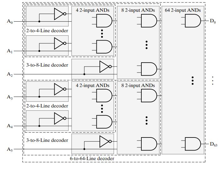
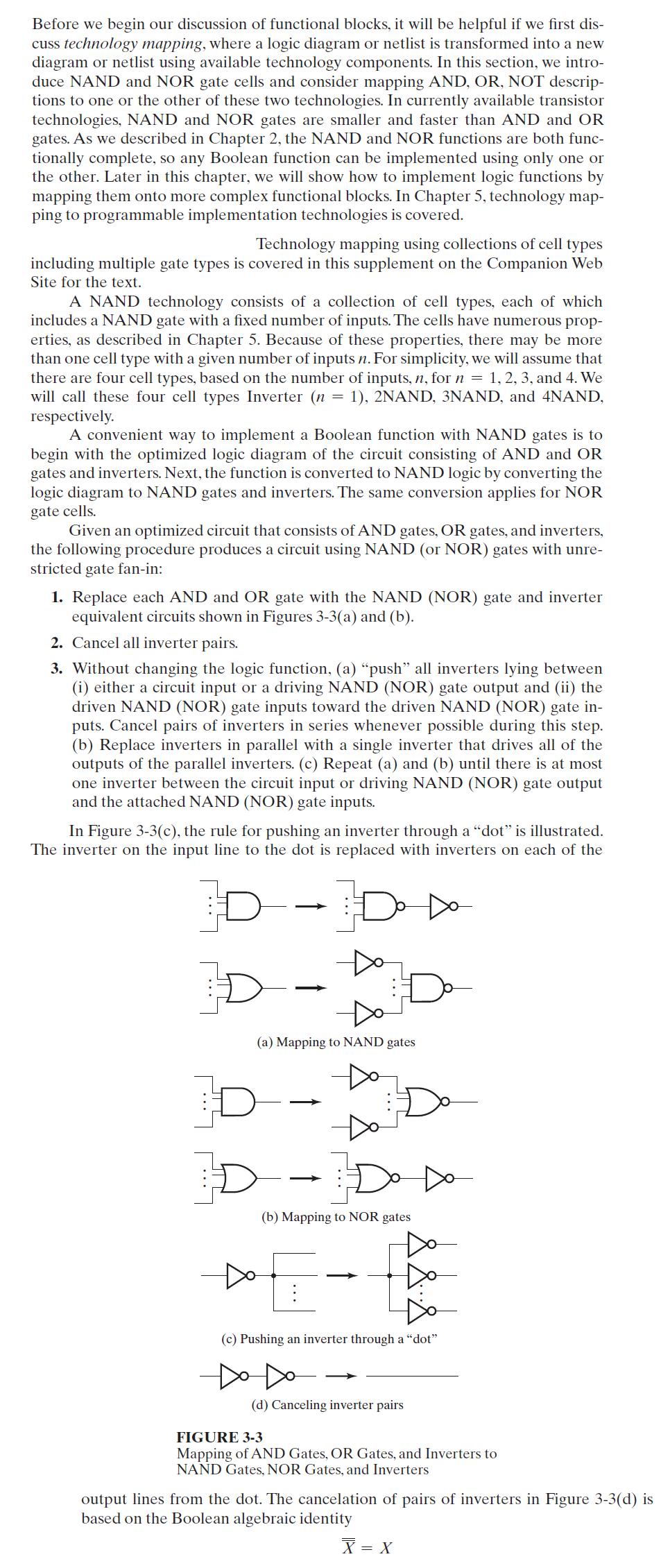
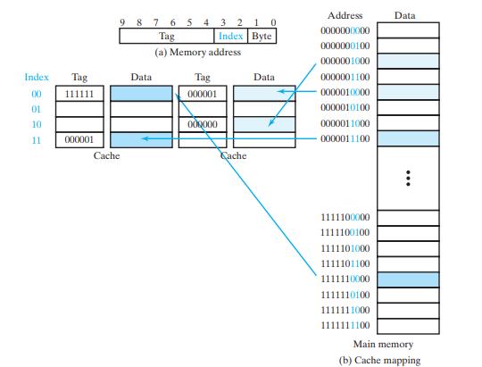
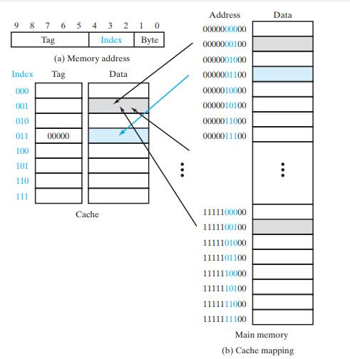
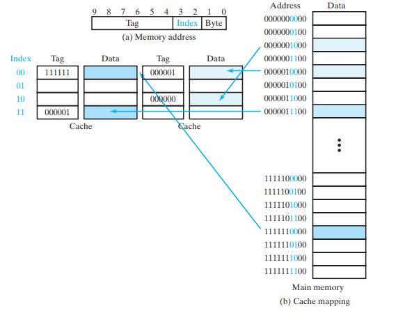
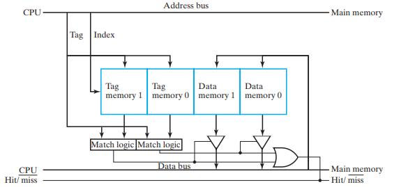
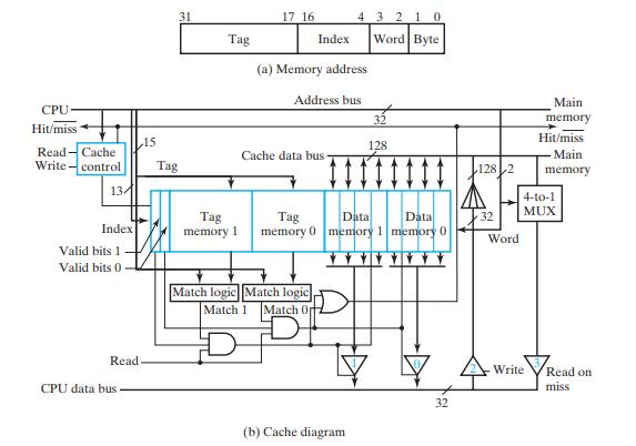
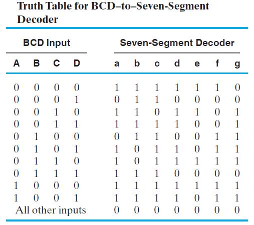
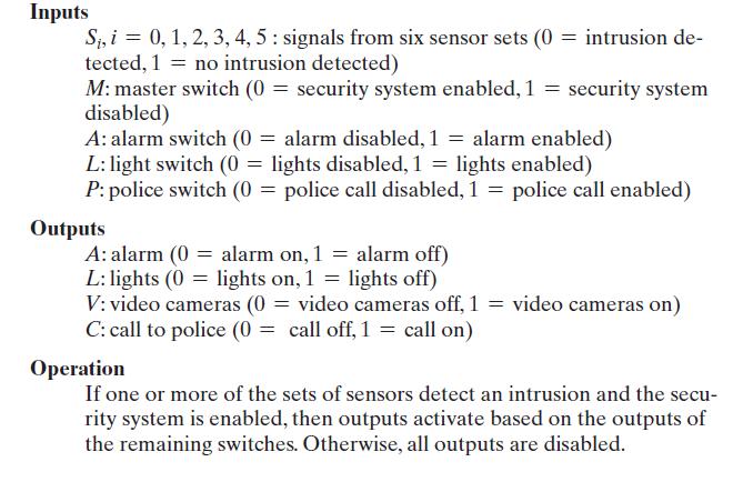
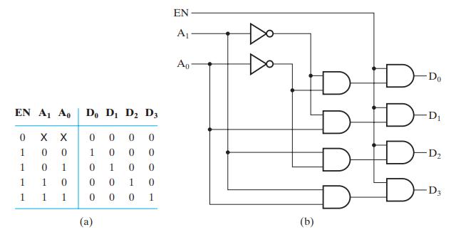
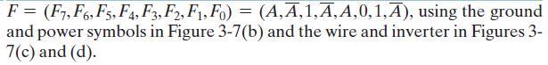
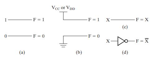
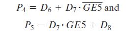
All Matches
Solution Library
Expert Answer
Textbooks
Search Textbook questions, tutors and Books
Oops, something went wrong!
Change your search query and then try again
Toggle navigation
FREE Trial
S
Books
FREE
Tutors
Study Help
Expert Questions
Accounting
General Management
Mathematics
Finance
Organizational Behaviour
Law
Physics
Operating System
Management Leadership
Sociology
Programming
Marketing
Database
Computer Network
Economics
Textbooks Solutions
Accounting
Managerial Accounting
Management Leadership
Cost Accounting
Statistics
Business Law
Corporate Finance
Finance
Economics
Auditing
Ask a Question
Search
Search
Sign In
Register
study help
computer science
logic and computer design fundamentals
Questions and Answers of
Logic And Computer Design Fundamentals
Find a function to detect an error in the representation of a decimal digit in BCD. In other words, write an equation with value 1 when the inputs are any one of the six unused bit combinations in
A trafic light control at a simple intersection uses a binary counter to produce the following sequence of combinations on lines A, B, C, and D: 0000, 0001, 0011, 0010, 0110, 0111, 0101, 0100, 1100,
Design a combinational circuit that accepts a 3-bit number and generates a 6-bit binary number output equal to the square of the input number.
Design a circuit with a 4-bit BCD input A, B, C, D that produces an output W, X, Y, Z that is equal to the input + 3 in binary. For example, 9 (1001) + 3 (0011) = 12 (1100). The outputs for invalid
A trafic metering system for controlling the release of trafic from an entrance ramp onto a superhighway has the following speciications for a part of its controller. There are three parallel
Design a circuit to implement the following pair of Boolean equations:To simplify drawing the schematic, the circuit is to use a hierarchy based on the factoring shown in the equation. Three
A hierarchical component with the function is to be used along with inverters to implement the following equation:The overall circuit can be obtained by using Shannon’s expansion theorem,where
Perform technology mapping to NAND gates for the circuit in Figure 3-54. Use cell types selected from: Inverter (n = 1), 2NAND, 3NAND, and 4NAND, as deined at the beginning of Section 3-2.Figure
Repeat Problem 3-16, using NOR gate cell types selected from: Inverter (n = 1), 2NOR, 3NOR, and 4NOR, each deined in the same manner as the corresponding four NAND cell types at the beginning of
(a) Repeat Problem 3-16 for the Boolean equations for the segments a and c of the BCD to seven-segment decoder from Example 3-18. Share common terms where possible.(b) Repeat part (a) using only
(a) Repeat Problem 3-18, mapping to NOR gate cell types as in Problem 3-17.Share common terms where possible.(b) Repeat part (a) using only Inverter (n = 1) and 2NOR cell types.Problem
Do Problem 3-21 by using logic simulation to find the output waveforms of the circuit or a partial truth-table listing, rather than finding Boolean functions.Problem 3-21The logic diagram for a
A special 4–to–6-line decoder is to be designed. The input codes used are 000 through 101. For a given code applied, the output Di, with i equal to the decimal equivalent of the code, is 1 and
An electronic game uses an array of seven LEDs (light-emitting diodes) to display the results of a random roll of a die. A decoder is to be designed to illuminate the appropriate diodes for the
Obtain the 1s and 2s complements of the following unsigned binary numbers: 10011100, 10011101, 10101000, 00000000, and 10000000.
sequential circuit with two D lip- lops A and B, two inputs X and Y, and one output Z is speciied by the following input equations:(a) Draw the logic diagram of the circuit.(b) Derive the state
A sequential circuit for a luggage lock has ten pushbuttons labeled 0, 1, 2, 3, 4, 5, 6, 7, 8, and 9. Each pushbutton 0 through 9 produces a 1 on Xi, i = 0 through 9, respectively, with all other
A serial 2s complementer is to be designed. A binary integer of arbitrary length is presented to the serial 2s complementer, least signiicant bit irst, on input X. When a given bit is presented on
The sequence in Problem 4-21 is a lag used in a communication network that represents the beginning of a message. This lag must be unique. As a consequence, at most ive 1s in sequence may appear
In many communication and networking systems, the signal transmitted on the communication line uses a non- return- to- zero (NRZ) format. USB uses a speciic version referred to as non- return- to-
Repeat Problem 4-27 with D lip- lops using a Gray- code assignment.Problem 4-27:A sequential circuit has two lip- lops A and B, one input X, and one output Y. The state diagram is shown in Figure
Design the register address logic in the pipelined CISC CPU by using information given in the register ields of Table 10-4 plus multiple-bit multiplexers, AND gates, OR gates, and inverters.Table 10-4
A CPU produces the following sequence of read addresses in hexadecimal:54, 58, 104, 5C, 108, 60, F0, 64, 54, 58, 10C, 5C, 110, 60, F0, 64.Supposing that the cache is empty to begin with, and assuming
Repeat Problem 12-1 for the following sequence of read addresses: 0, 4, 12, 8, 14, 1C, 1A, 28, 26, 2E, 36, 30, 3E 38, 46, 40, 4E, 48, 56, 50, 5E, 58.Problem 12-1A CPU produces the following sequence
A computer has a 32-bit address and a direct-mapped cache. Addressing is to the byte level. The cache has a capacity of 1 KB and uses lines that are 32 bytes. It uses write-through and so does not
A two-way set-associative cache in a system with 32-bit addresses has four 4-byte words per line and a capacity of 1 MB. Addressing is to the byte level.(a) How many bits are there in the index and
Discuss the advantages and disadvantages of:(a) Instruction and data caches versus a unified cache for both.(b) Write-back cache versus a write-through cache.
Give an example of a sequence of program and data memory read addresses that will have a high hit rate for separate instruction and data caches and a low hit rate for a unified cache. Assume
Give an example of a sequence of program and data memory read addresses that will have a high hit rate for a unified cache and a low hit rate for separate instruction and data caches. Assume that
Explain why write-allocate is typically not used in a write-through cache.
A 1 KB cache in a system with 32-bit addresses using byte addressing is organized using four 4-byte words per line and direct mapping.(a) How many sets are in the cache?(b) How many bits are in the
A high-speed workstation has 64-bit words and 64-bit addresses with address resolution to the byte level.(a) How many words can be in the address space of the workstation?(b) Assuming a
A cache memory has an access time from the CPU of 4 ns, and the main memory has an access time from the CPU of 40 ns. What is the effective access time for the cache–main memory hierarchy if the
Repeat Problem 12-11 if the cache access time from the CPU is 1 ns and the main memory has an access time from the CPU of 20 ns.Problem 12-11A cache memory has an access time from the CPU of 4 ns,
Redesign the cache in Figure 12-7 so that it is the same size, but is four-way set associative rather than two-way set associative.Figure 12-7 CPU CPU Hit/ miss Tag Index Address bus Tag Tag Data
The cache in Figure 12-9 is to be redesigned to use write-back with write allocate rather than write-through. Respond to the following requests, making sure to deal with all of the address and data
A virtual memory system uses 4 KB pages, 64-bit words, and a 48-bit virtual address. A particular program and its data require 4263 pages.(a) What is the minimum number of page tables
A computer uses 64-bit virtual addresses, 32-bit words, and a page size of 4 KB. The computer has 1 GB of physical memory.(a) How many bits of the address are used for the page offset?(b) How many
A small TLB has the following entries for a virtual page number of length 20 bits, a physical page number of 12 bits, and a page offset of 12 bits.The page numbers and offset are given in
A computer can accommodate a maximum of 384 MB of main memory. It has a 32-bit word and a 32-bit virtual address and uses 4 KB pages. The TLB contains only entries that include the Valid, Dirty, and
Four programs are concurrently executing in a multitasking computer with virtual memory pages having 4 KB. Each page table entry is 32 bits. What is the minimum numbers of bytes of main memory
In caches, we use both write-through and write-back as potential writing approaches. But for virtual memory, only an approach that resembles writeback is used. Give a sound explanation of why this is
Explain clearly why both the cache memory concept and the virtual memory concept would be ineffective if locality of reference of memory-addressing patterns did not hold.
By using manual methods, verify that the circuit of Figure 3-55 generates the exclusive-NOR function.Figure 3-55 X Y Do -F
(a) Use logic simulation to verify that the circuits described in Example 3-18 implement the BCD–to–seven-segment converter correctly.(b) Design the converter assuming that the unused input
Complete the design of the BCD–to–seven-segment decoder by performing the following steps:(a) Plot the seven maps for each of the outputs for the BCD–to–sevensegment decoder speciied in
Repeat Problem 3-4 for 4 x 4 tic-tac-toe, which is played on a four-by-four grid. Assume that the numbering pattern is left to right and top to bottom, as in Problem 3-4.Problem 3-4A simple
A simple well-known game, tic-tac-toe, is played on a three-by-three grid of squares by two players. The players alternate turns. Each player chooses a square and places a mark in a square. (One
A majority function has an output value of 1 if there are more 1s than 0s on its inputs. The output is 0 otherwise. Design a three-input majority function.
A home security system has a master switch that is used to enable an alarm, lights, video cameras, and a call to local police in the event one or more of six sets of sensors detects an intrusion. In
Design a Gray code–to–BCD code converter that gives output code 1111 for all invalid input combinations. Assume that the Gray code sequence for decimal numbers 0 through 9 is 0000, 0001, 0011,
A low-voltage lighting system is to use a binary logic control for a particular light. This light lies at the intersection point of a T-shaped hallway. There is a switch for this light at each of the
Design a combinational circuit that accepts a 4-bit number and generates a 3-bit binary number output that approximates the square root of the number. For example, if the square root is 3.5 or
The logic diagram for a 74HC138 MSI CMOS circuit is given in Figure 3-56. Find the Boolean function for each of the outputs. Describe the circuit function carefully.Figure 3-56 A B C- G GA GB 8 8 -
A NAND gate with eight inputs is required. For each of the following cases, minimize the number of gates used in the multiple-level result:(a) Design the 8-input NAND gate using 2-input NAND gates
(a) Draw an implementation diagram for a constant vector function F = (F7, F6, F5, F4, F3, F2, F1, F0) = (1, 0, 0, 1, 0, 1, 1, 0) using the ground and power symbols in Figure 3-7(b).(b) Draw an
Design a 4–to–16-line decoder with enable using ive 2–to–4-line decoders with enable as shown in Figure 3-16.Figure 3-16. EN A Ao 0 X X 1 0 1 1 1 1 00x 1 0 1 1 Do D D D3 0 0 0 0 0 0 1 0 0 0 1
(a) Draw an implementation diagram for rudimentary vector function (b) and the wire and inverter in Figures 3-7 (c) and (d).Figure 3-7 F = (F7, F6,F5, F4, F3, F2, F1, F0) = (A,A,1,A,A,0,1,A),
To provide uphill running and walking, an exercise treadmill has a grade feature that can be set from 0.0% to 15.0% in increments of 0.1%. (The grade in percent is the slope expressed as a
(a) Draw an implementation diagram for the vector G = (G5 , G4 , G3 , G2 , G1, G0) = (F13, F8, F5, F3, F2, F1).(b) Draw a simple implementation for the rudimentary vector H = (H7, H6, H5, H4, H3,
Design a 4–to–16-line decoder using two 3–to–8-line decoders and 16 2-input AND gates.
Design a 5–to–32-line decoder using a 3–to–8-line decoder, a 2–to–4-line decoder, and 32 2-input AND gates.
Draw the detailed logic diagram of a 3–to–8-line decoder using only NOR and NOT gates. Include an enable input.
Design a 4-input priority encoder with inputs and outputs as in Table 3-6, but with the truth table representing the case in which input D0 has the highest priority and input D3 the lowest
Derive the truth table of a decimal-to-binary priority encoder. There are 10 inputs I1 through I9 and outputs A3 through A0 and V. Input I9 has the highest priority.
(a) Design an 8–to–1-line multiplexer using a 3–to–8-line decoder and an 8 х 2 AND-OR.(b) Repeat part (a), using two 4–to–1-line multiplexers and one 2-to-1-line multiplexer.
Design a 16–to–1-line multiplexer using a 4–to–16-line decoder and a 16 х 2 AND-OR.
Design a dual 8–to–1-line decoder using a 3–to–8-line decoder and two 8 х 2 AND-ORs.
Rearrange the condensed truth table for the circuit of Figure 3-16, and verify that the circuit can function as a demultiplexer.Figure 3-16 EN A Ao Do D D D3 0 X X 0 0 0 1 0 1 0 0 1 1 1 1 1 0 1 0 1 0
Construct a 12–to–1-line multiplexer with a 3–to–8-line decoder, a 1–to–2- line decoder, and a 12 х 3 AND-OR. The selection codes 0000 through 1011 must be directly applied to the
The rear lights of a car are to be controlled by digital logic. There is a single lamp in each of the rear lights.(a) Write the equations for LR and RR. Assume that BR overrides EM and that LT and
Construct a quad 10–to–1-line multiplexer with four single 8–to–1-line multiplexers and two quadruple 2–to–1-line multiplexers. The multiplexers should be interconnected and inputs
Construct a 15–to–1-line multiplexer with two 8–to–1-line multiplexers. Interconnect the two multiplexers and label the inputs such that any added logic required to have selection codes 0000
Implement the Boolean functionwith a 4–to–1-line multiplexer and external gates. Connect inputs A and B to the selection lines. The input requirements for the four data lines will be a function
A combinational circuit is deined by the following three Boolean functions:Design the circuit with a decoder and external OR gates. F = X+Z+ XYZ F = X + Z + XYZ F3 = XYZ + X+Z
Solve Problem 3-47 using two 3–to–8-line decoders with enables, an inverter, and OR gates with a maximum fan-in of 4.Problem 3-47Implement the Boolean functionwith a 4–to–1-line multiplexer
Implement the following Boolean function with an 8–to–1-line multiplexer and a single inverter with variable D as its input: F(A, B, C, D) = m(2, 4, 6, 9, 10, 11, 15)
The logic diagram of the first stage of a 4-bit adder, as implemented in integrated circuit type 74283, is shown in Figure 3-58. Verify that the circuit implements a full adder.Figure 3-58 Bo Ao TD
Design a combinational circuit that forms the 2-bit binary sum S1S0 of two 2-bit numbers A1A0 and B1B0 and has both a carry input C0 and carry output C2. Design the entire circuit implementing each
The adder–subtractor circuit of Figure 3-45 has the following values for input select S and data inputs A and B:Figure 3-45 Determine, in each case, the values of the outputs S3, S2, S1, S0, and
Using Figure 3-28 as a guide, write a structural VHDL description for the full-adder circuit in Figure 3-58. Compile and simulate your description. Apply all eight input combinations to check the
Perform the indicated subtraction with the following unsigned binary numbers by taking the 2s complement of the subtrahend:(a) 11010 - 10001(b) 11110 - 1110(c) 1111110 - 1111110(d) 101001 - 101
Repeat Problem 3-52, assuming the numbers are 2s complement signed numbers. Use extension to equalize the length of the operands. Indicate whether overflow occurs during the complement operations for
Perform the arithmetic operations (+36) + (-24) and (-35) - (-24) in binary using signed 2s complement representation for negative numbers.
The following binary numbers have a sign in the leftmost position and, if negative, are in 2s complement form. Perform the indicated arithmetic operations and verify the answers.(a) 100111 +
Design two versions of the combinational circuit whose input is a 4-bit number and whose output is the 2s complement of the input number, for each of the following cases using AND, OR, and NOT
Using Figure 3-31 as a guide, write a structural Verilog description for the fulladder circuit in Figure 3-58. Compile and simulate your description. Apply all eight input combinations to check the
Compile and simulate the 4-bit adder in Figures 3-47 and 3-48. Apply combinations that check out the rightmost full adder for all eight input combinations; this also serves as a check for the other
Use contraction beginning with a 4-bit adder with carry out to design a 4-bit increment-by-2 circuit with carry out that adds the binary value 0010 to its 4-bit input. The function to be implemented
Use contraction beginning with an 8-bit adder–subtractor without carry out to design an 8-bit circuit without carry out that increments its input by 000000101 for input S = 0 and decrements its
Design a combinational circuit that compares two 4-bit unsigned numbers A and B to see whether B is greater than A. The circuit has one output X, so that X = 1 if A < B and X = 0 if A ≥ B.
Using Figure 3-49 as a guide and a “when-else” on S from Figure 3-29, write a high-level behavior VHDL description for the adder–subtractor in Figure 3-46 (see Figure 3-45 for details). Compile
Repeat Problem 3-59 by using three-input, one-output circuits, one for each of the four bits. The four circuits are connected together in cascade by carrylike signals. One of the inputs to each cell
Compile and simulate the behavioral description of the 4-bit adder in Figure 3-49. Assuming a ripple carry implementation, apply combinations that check out the rightmost full adder for all eight
Repeat Problem 3-59 by applying contraction to a 4-bit subtractor and using the borrow out as X.Problem 3-59Design a combinational circuit that compares two 4-bit unsigned numbers A and B to see
Design a combinational circuit that compares 4-bit unsigned numbers A and B to see whether A = B or A > B. Use an iterative circuit as in Problem 3-60.Problem 3-60Repeat Problem 3-59 by using
Design a 5-bit signed-magnitude adder–subtractor. Divide the circuit for design into (1) sign generation and add–subtract control logic, (2) an unsigned number adder–subtractor using 2s
Using Figure 3-51 as a guide and a “binary decision” on S from Figure 3-34, write a high-level behavior Verilog description for the adder–subtractor in Figure 3-46 (see Figure 3-45 for
Perform a manual or computer- based logic simulation similar to that given in Figure 4-5 for the SR latch with control input C in Figure 4-7. In particular, examine the behavior of the circuit when S
Compile and simulate the 4-bit adder in Figure 3-50. Apply combinations that check out the rightmost full adder for all eight input combinations; this also serves as a check for the other full
Showing 1 - 100
of 412
1
2
3
4
5