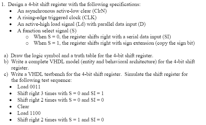
Question: 1. Design a 4-bit shift register with the following specifications: An asynchronous active-low clear (CliN) A rising-edge triggered clock (CLK) An active-high load signal (Ld)

1. Design a 4-bit shift register with the following specifications: An asynchronous active-low clear (CliN) A rising-edge triggered clock (CLK) An active-high load signal (Ld) with parallel data input (D) A function select signal (S) o When S = 0, the register shifts right with a serial data input (SI) o When S = 1, the register shifts right with sign extension (copy the sign bit) a) Draw the logic symbol and a truth table for the 4-bit shift register. b) Write a complete VHDL model (entity and behavioral architecture) for the 4-bit shift register. c) Write a VHDL testbench for the 4-bit shift register. Simulate the shift register for the following test sequence: Load 0011 Shift right 3 times with S = 0 and SI = 1 Shift right 2 times with S = 0 and SI = 0 Clear Load 1100 Shift right 2 times with S = 1 and SI = 0
Step by Step Solution
There are 3 Steps involved in it

Get step-by-step solutions from verified subject matter experts


