

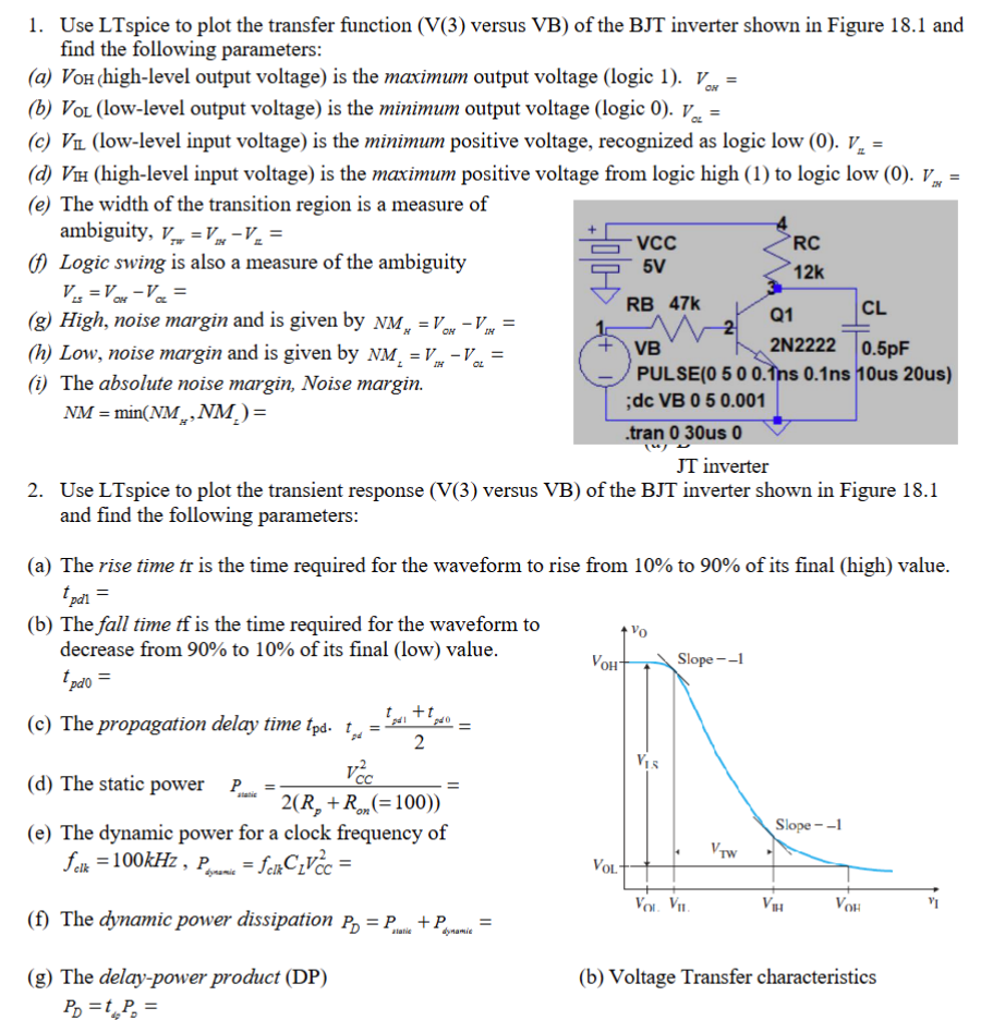
Question: 1 . Use LTspice to plot the transfer function ( V ( 3 ) versus VB ) of the BJT inverter shown in Figure 1
Use LTspice to plot the transfer function V versus VB of the BJT inverter shown in Figure and find the following parameters: a V OH highlevel output voltage is the maximum output voltage logic V OF b V OL lowlevel output voltage is the minimum output voltage logic V OL c V IL lowlevel input voltage is the minimum positive voltage, recognized as logic low VmathbbRd V IH highlevel input voltage is the maximum positive voltage from logic high to logic low V ar e The width of the transition region is a measure of ambiguity, V IW V IW V IL f Logic swing is also a measure of the ambiguity V LS V ott V ot VCC V RB k VB RC k Qg High, noise margin and is given by NM R V ort V or h Low, noise margin and is given by NMLV Rt V ot N CL pF i The absolute noise margin, Noise margin. PULSEns ns us us NM minNMy NMz ;dc VB tran us JT inverter Use LTspice to plot the transient response V versus VB of the BJT inverter shown in Figure and find the following parameters: a The rise time tr is the time required for the waveform to rise from to of its final high value. I pdb The fall time tf is the time required for the waveform to decrease from to of its final low value. t pd Slope V perp s c The propagation delay time tpd t pd t pdt pdd The static power P oue V CC R p R on e The dynamic power for a clock frequency of
Step by Step Solution
There are 3 Steps involved in it
1 Expert Approved Answer
Step: 1 Unlock

Question Has Been Solved by an Expert!
Get step-by-step solutions from verified subject matter experts
Step: 2 Unlock
Step: 3 Unlock