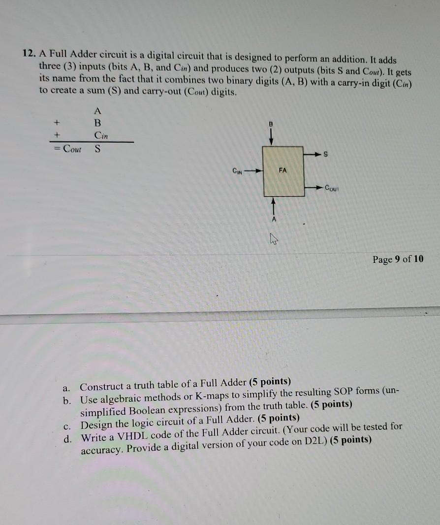
Question: 12. A Full Adder circuit is a digital circuit that is designed to perform an addition. It adds three (3) inputs (bits A, B,

12. A Full Adder circuit is a digital circuit that is designed to perform an addition. It adds three (3) inputs (bits A, B, and Cin) and produces two (2) outputs (bits S and Cout). It gets its name from the fact that it combines two binary digits (A, B) with a carry-in digit (Cin) to create a sum (S) and carry-out (Cout) digits. A B Cin + + = Cout S GIN FA -S -Cout Page 9 of 10 a. Construct a truth table of a Full Adder (5 points) b. Use algebraic methods or K-maps to simplify the resulting SOP forms (un- simplified Boolean expressions) from the truth table. (5 points) c. Design the logic circuit of a Full Adder. (5 points) d. Write a VHDL code of the Full Adder circuit. (Your code will be tested for accuracy. Provide a digital version of your code on D2L) (5 points)
Step by Step Solution
There are 3 Steps involved in it
Full Adder truth table simplifying Boolean expressions designing a logic circuit and writing VHDL co... View full answer

Get step-by-step solutions from verified subject matter experts


