

Question: B.3 A BCD-to-binary converter circuit is implemented using a 256 x 7 ROM as shown in Figure B.3. The X-input is the tens digit (most
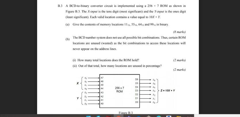
B.3 A BCD-to-binary converter circuit is implemented using a 256 x 7 ROM as shown in Figure B.3. The X-input is the tens digit (most significant) and the Y-input is the ones digit (least significant). Each valid location contains a value equal to 10X + Y. (a) Give the contents of memory locations 111.551., 641 and 996 in binary (8 marks) (b) The BCD number system does not use all possible bit combinations. Thus, certain ROM locations are unused (wasted) as the bit combinations to access these locations will never appear on the address lines. (2 marks) (0) How many total locations does the ROM hold? (i) Out of that total, how many locations are unused in percentage? (2 marks) X M1 Xo AY A6 A5 A4 A3 A2 A1 D6 05 04 D3 D2 D1 DO NNN 256 x 7 ROM Z = 10x +Y 21 20 yo Figure B3
Step by Step Solution
There are 3 Steps involved in it

Get step-by-step solutions from verified subject matter experts